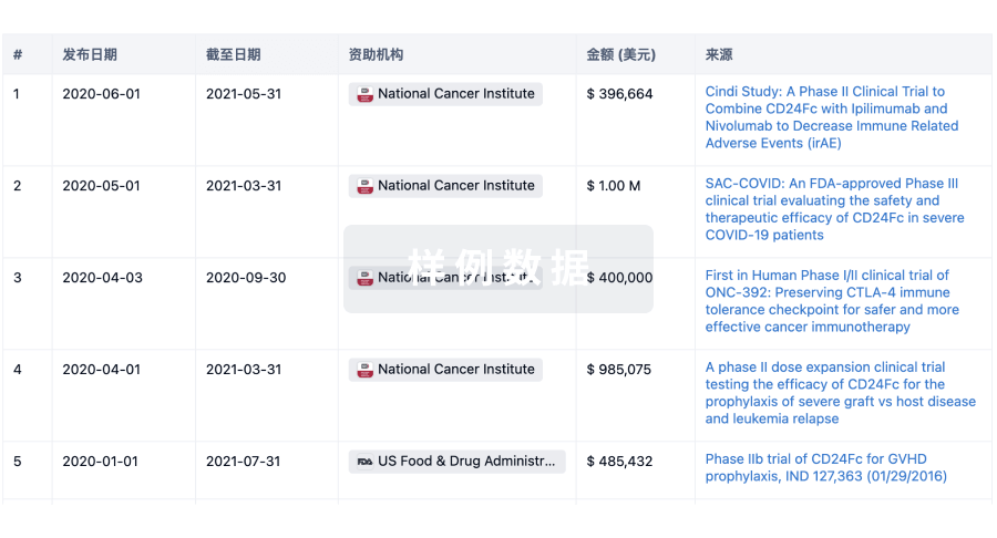
This paper presents integrated sensing and computing memory (ISCM) devices based on V2O5/WO3 heterostructures using wafer-scalable semiconductor microfabrication processes.The impact of the V2O5/WO3 heterostructure-based ISCM devices was tested and compared with the V2O5- and WO3-based ISCM structures.The heterostructured devices have broadband sensing capability with improved performance metrics as compared to the single-material-based ISCM devices.The heterostructured device has shown responsivity (1.5 A/W) and detectivity (1.2 x 10¹¹ Jones) at 950 nm.All fabricated devices were stimulated using AC and DC stimuli under various illumination conditions.The heterostructured ISCM device offers a high current switching ratio (30.6), and this value is 2 times and 17 times higher than WO3 and V2O5, resp.In addition, all devices have ultrafast resistive switching capability and long-term stability of >102 cycles.The heterostructured device has shown the set and reset times of 88.6/35.7 μs, resp., at 950 nm.In addition, the AND gate logic circuit is realized using elec. and optical stimuli.These test results have proven that the fabricated devices can be deployed as sensing/storage devices for future broadband sensing and memory technol.