预约演示
更新于:2026-06-06

Flex Ltd.
更新于:2026-06-06
概览
关联
100 项与 Flex Ltd. 相关的临床结果
登录后查看更多信息
0 项与 Flex Ltd. 相关的专利(医药)
登录后查看更多信息
4
项与 Flex Ltd. 相关的文献(医药)2011-03-21·ECS transactions
Failure Mechanism and Testing of PCB Pad Cratering
作者: Shangguan, Dongkai ; Cai, Miao ; Geiger, David ; Xie, Dongji ; Wu, Boyi ; Martin, Ivan
Pad cratering of printed circuit board (PCB) is becoming a prevailing issue encountered in the PCB assemblies which is accelerated when switching to leadfree process. These units with pad cratering may not fail during functional test as and raise potential failure in the field. This paper uses both experimental and finite element analysis (FEA) approaches to understand the pad strength and pad stresses. An extensive mechanical test by pin pull tests are performed on PCB materials. Cohesive elements are employed to simulate the bonding at the interfaces of pad, laminate and fibers. The results from FEA show that the laminate cracking can be successfully simulated. The design variables such as traces and solder fillet impact are also critical for pad cratering.
2002-12-05·ELECTRONICS LETTERS
Semi-insulating buried heterostructure laser with PN fence
作者: White, J.K. ; Pakulski, G. ; Knight, G. ; Jones, T. ; Blaauw, C. ; Das, S.R.
The design, fabrication, and performance, of an Fe-doped InP semiinsulating buried heterostructure laser using a PN fence that prevents Zn and Fe interdiffusion is described.
2002-11-01·Journal of Optics A: Pure and Applied Optics
Flexible polymer waveguides for optical wire bonds
作者: Clayton, Richard ; Robinson, Jason ; Clark, Cynthia
Low-loss flexible polyimide waveguides have been fabricated and optoelectronic components have been successfully connected together using these waveguides.The waveguides were fabricated from com. available polyamic acid and heat cured to form polyimide.Low bulk material absorption of the core polymer was measured in the 1300-1600 nm range.A processing technique which produced buried core waveguides removable from a Si wafer was developed.Low (2 dB cm-1) fiber-to-fiber losses of flexible waveguides were measured.A novel optical wire bonding technique which removed flexible waveguides from a Si wafer and connected them to optoelectronic chip facets is successful.
57
项与 Flex Ltd. 相关的新闻(医药)2026-06-05
Including United's offer for Spirit customers, eBay's response to GameStop's acquisition proposal, and a new partnership between major telecom providers.Plus, a recap of May's trending topics, including Memorial Day and Mother's Day.
NEW YORK, June 5, 2026 /PRNewswire/ -- With thousands of press releases published each month, it can be difficult to keep up with everything on PR Newswire. To help journalists and consumers stay on top of the month's most newsworthy and popular releases, here's a recap of some major stories from the last month that shouldn't be missed.
The list below includes the headline (with a link to the full text) and an excerpt from each story. Click on the press release headlines to access accompanying multimedia assets that are available for download.
Continue Reading
PR Newswire Monthly Press Release Roundup, May 2026. Photos provided by United Airlines, Kentucky Fried Chicken and Novo Nordisk.
United Offers Support for Spirit Airlines Customers and Employees
On May 2, the United Airlines press release said, "If you had a ticket booked on Spirit and your flight was canceled, for the next two weeks you can visit united.com/specialfares to find price-capped, one-way tickets from most cities where Spirit flew, including Atlanta, Chicago, Fort Lauderdale, Houston, Las Vegas, Miami, Newark, New Orleans and Orlando."
eBay Rejects Unsolicited Proposal from GameStop
"With its differentiated global marketplace and a clear strategy, eBay's Board is confident that the company, under its current management team, is well-positioned to continue to drive sustainable growth, execute with discipline, and deliver long-term value for our shareholders," the statement said.
Lilly's triple agonist, retatrutide, delivered powerful weight loss in pivotal Phase 3 obesity trial
In TRIUMPH-1, participants on 12 mg retatrutide lost an average of 70.3 lbs (28.3%) over 80 weeks with 45.3% of participants achieving ≥30% weight loss, a level long associated with bariatric surgery.
AT&T, T-Mobile, and Verizon Plan to Launch New Joint Venture that Helps End Dead Zones
The Joint Venture will accelerate American leadership in next-generation direct-to-device (D2D) communications by using satellite-based technologies to address coverage gaps, especially in unserved and underserved communities.
Allegiant Adds Eight New Nonstop Routes, Expanding Service to Florida
The new routes, beginning in fall 2026, will provide convenient, nonstop service and expand Allegiant's growing presence in leisure destinations across Florida.
KFC® Expands $10 Tuesday into a Weekday Bucket Lineup, Introduces Two New Sauces
With four different bucket meals all priced at just $10, including the nuggets bucket returning Friday to round out the week, the lineup delivers unbeatable value worth jumping on while it lasts.
Novo Nordisk's Ozempic® pill, the only FDA-approved oral peptide GLP-1 medication for adults with type 2 diabetes, soon to be available in the US
"With Ozempic® now available as both an injection and oral option under one brand, treatment can be individualized so patients are getting the proven semaglutide medicine that best fits their needs," said Ed Cinca, senior vice president of Marketing & Patient Solutions at Novo Nordisk Inc.
NextEra Energy and Dominion Energy to Combine, Creating the World's Largest Regulated Electric Utility Business and North America's Premier Energy Infrastructure Platform Benefiting Customers
The combined company will be more than 80% regulated, serve approximately 10 million utility customer accounts across Florida, Virginia, North Carolina and South Carolina and own 110 gigawatts (GW) of generation across a broad mix of energy sources.
Hisense Unveils XR10: The Apex of Projector, Bringing Cinema Into Every Home
With 6,000 ANSI lumens, XR10 ensures bright, vivid visuals even in well-lit spaces, so users can enjoy clear, lifelike images from morning news to late-night movies—no need to dim the room.
Cracker Barrel Launches "Fuel Your Summer Road Trip" With $250,000 in Free Gas and Homestyle Cooking
From May 19 through July 26, 250 lucky Cracker Barrel Rewards members will each win $1,000 total (a $500 Cracker Barrel gift card and a $500 gas gift card) to use toward road trips, weekend getaways or everyday summer travel - that's 25 new winners each week.
Flex Announces Intention to Spin Off its Cloud and Power Infrastructure Segment into a New Independent Publicly Traded Company
The new company will be a high-growth critical digital and electrical infrastructure company, delivering end-to-end power and thermal management technologies and integrated infrastructure systems for AI data centers and mission-critical applications.
Honeywell Announces Quantinuum's Filing of Registration Statement for Proposed Initial Public Offering
Quantinuum intends to list its Class A common stock on the Nasdaq Global Select Market under the ticker symbol "QNT."
Shell Introduces Credit Card That Rewards Everyday Spending Beyond Fuel
The Shell Performance Elite World Mastercard is designed to maximize value from how customers already spend, helping them earn more across fuel, EV charging, groceries, dining, and all other purchases.
Read more of the latest releases from PR Newswire.
Trending Topics
In addition to the newsworthy headlines above, the PR Newswire team spotted several larger trending topics dominating headlines in May:
Memorial Day
: As the unofficial start of summer approached, many brands distributed releases for their holiday product launches and deals, events, and more. Announcements ranged from deals on summer snack favorites to discoveries of U.S. WWII lost vessels, various events to honor the U.S. military, and the kick-off for a summer full of America250 celebrations.
Mother's Day
: Brands in the consumer/retail, health, tech and other industries shared how they were celebrating moms ahead of the mid-May holiday. Campaigns celebrated the strength of NICU moms, supported those who have lost a mother or mother-figure, advocated for more awareness of Perinatal Mental Health Disorders, and even recognized mothers' role as the first financial coach for many Americans.
Earnings
: The latest earnings period wound down in mid-May, with quarterly results from Target, Cisco, Lowe's, GoPro and many more sent via PR Newswire.
Coming Up: In June, the team is expecting increases in releases tied to Pride Month, Juneteenth and the FIFA World Cup. Plus, as the Fourth of July and America's 250th birthday approach, many brands will be sharing their related news, from event details to sales, product launches and beyond.
Do you have a press release to distribute? Sign up with PR Newswire to share your story with the audiences who matter most.
Helping Journalists Stay Up to Date on Industry News
These are just a few of the recent press releases that consumers and the media should know about. To be notified of releases relevant to their coverage area, journalists can set up a custom newsfeed with PR Newswire for Journalists.
Once they're signed up, reporters, bloggers, and freelancers have access to the following
free features:
Customization: Users can create customized newsfeeds that will deliver relevant news right to their inbox. Newsfeed results can be targeted by keywords, industry, subject, geography, and more.
Photos and Videos: Thousands of multimedia assets are available to download and include in a journalist or blogger's next story.
Subject Matter Experts: Journalists will have access to ProfNet, a database of industry experts to connect with as sources or for quotes in their articles.
Related Resources: Our journalist- and blogger-focused blog, Beyond Bylines, features regular media news roundups, writing tips, upcoming events, and more.
About PR Newswire
PR Newswire is the industry's leading press release distribution partner with an unparalleled global reach of more than 500,000 newsrooms, websites, direct feeds, journalists and influencers and is available in more than 170 countries and 40 languages. From our innovative AI-powered PR Newswire Amplify™ platform, award-winning Content Services offerings, integrated media newsroom and microsite products, Investor Relations suite of services, paid placement and social sharing tools, PR Newswire has a comprehensive Multichannel Amplification™ catalogue of solutions to solve the modern-day challenges PR and communications teams face. For more than 70 years, PR Newswire has been the preferred destination worldwide for brands to share their most important news stories.
For questions, contact the team at [email protected].
SOURCE PR Newswire
21%
more press release views with
Request a Demo
并购临床3期临床结果
2026-06-05
CAMBRIDGE, England--(BUSINESS WIRE)--Cycle Pharmaceuticals (Cycle) announces the FDA approval of CAVHANZA (nilotinib) Orally Disintegrating Tablets. Launching soon, the CAVHANZA formulation is specifically designed to improve solubility and dissolution rate, enabling maintained bioavailability with concomitant use of acid-reducing agents such as proton pump inhibitors (PPIs) and/or H₂ antagonists (H₂RAs) without timing restrictions.1
This is a first in the nilotinib landscape, addressing a known challenge in Philadelphia chromosome-positive chronic myeloid leukemia (Ph+ CML) treatment.
This will be a first in the nilotinib market, addressing a known challenge in Philadelphia chromosome-positive chronic myeloid leukemia (Ph+ CML) treatment, where 25% of patients are co-prescribed PPIs or H₂RAs – medications that can compromise treatment efficacy.3 In clinical trials, CAVHANZA demonstrated no food effect and can be taken without regard to meals, reducing food-related burden and supporting more flexible dosing, potentially improving treatment outcomes.1,2,4 Additionally, as an orally disintegrating tablet, CAVHANZA may support patients who have difficulty swallowing while also offering flexibility to take the treatment with or without water.1
CAVHANZA is indicated for the treatment of:
Newly diagnosed adults with Ph+ CML in chronic phase; and 1
Adults with chronic and accelerated phase Ph+ CML with resistance or intolerance to prior therapy, including imatinib. 1
“We’re excited to be able to offer the CML community another TKI option that may better suit their needs,” said Victoria Dickinson, Chief Product Officer at Cycle. “Finding the right treatment that fits a patient’s needs and lifestyle can be a stressful step in a patient’s treatment journey. Bringing another option to market – backed by Cycle VitaTM, our dedicated patient support* program – is an exciting prospect for Cycle.”
To prepare CAVHANZA for market, Cycle partnered with Flex Pharma (Flex), who specialize in advanced formulation solutions and has developed an improved formulation of the second-generation TKI – built on years of established nilotinib efficacy.
Christian Wertz, PhD, President of Flex, added “This collaboration reflects Flex’s strategy as a technology-driven company advancing differentiated 505(b)(2) oncology therapies. Leveraging our proprietary ElectroNanoSpray™ (ENS) platform, we reformulate established oncology molecules to enhance bioavailability and optimize dosing performance. Together with Cycle’s rare-disease commercialization expertise, we aim to efficiently deliver improved treatment options for patients with rare leukemias.”
Cycle has been delivering patient-focused treatments since 2017. The approval, and upcoming launch, of CAVHANZA represents the 10th product in Cycle's portfolio and the 2nd product to enhance treatment options for patients living with Ph+ CML.
Learn more about CAVHANZA at https://cyclepharma.com/chronic-myeloid-leukemia-new-treatment.
Warning: QT Prolongation and Sudden Deaths
Nilotinib prolongs the QT interval. Monitor for hypokalemia or hypomagnesemia and correct deficiencies. Obtain ECGs to monitor the QTc at baseline on day 7, and periodically thereafter, and following any dose adjustments.
Sudden deaths have been reported. Avoid use in patients with hypokalemia, hypomagnesemia or long QT syndrome.
Avoid concomitant drug use with QT-prolonging drugs and strong CYP3A4 inhibitors.
Indications
CAVHANZA (nilotinib) is a kinase inhibitor indicated for the treatment of:
Adult patients with newly diagnosed Philadelphia chromosome positive chronic myeloid leukemia (Ph+ CML) in chronic phase (CP).
Adults with CP Ph+ CML or accelerated phase (AP) Ph+ CML resistant to or intolerant to prior therapy.
Contraindications
CAVHANZA is contraindicated in patients with hypokalemia, hypomagnesemia, or long QT syndrome.
Important Safety Information
Warnings and Precautions:
Substitution between nilotinib products requires dose conversion to avoid medication errors.
Monitor for myelosuppression; manage with dose adjustments or interruptions.
Cardiovascular and arterial occlusive events have been reported; assess and monitor cardiovascular risk.
Pancreatitis risk: monitor serum lipase; interrupt dosing if abdominal symptoms occur with lipase elevations.
Hepatotoxicity has been reported, with higher risk in pediatrics. Monitor liver function tests regularly.
Correct and monitor electrolyte abnormalities throughout treatment.
Tumor lysis syndrome has been reported; ensure hydration and correct uric acid before initiating treatment.
Serious hemorrhage may occur; advise patients to report signs and symptoms of bleeding.
Monitor for fluid retention and manage accordingly.
Growth retardation has been reported in pediatric patients. Monitor growth and development.
Can cause fetal harm; advise use of effective contraception during and 14 days after treatment.
Monitor BCR-ABL transcript levels in patients discontinuing treatment and manage loss of response appropriately.
Adverse Reactions:
Common non-hematologic adverse reactions include rash, pruritus, headache, nausea, fatigue, alopecia, myalgia, abdominal pain, constipation, diarrhea and vomiting. Hematologic adverse reactions include thrombocytopenia, neutropenia, and anemia. Serious adverse reactions include QT prolongation, sudden deaths, febrile neutropenia, and intracranial hemorrhage. Postmarketing reports include thrombotic microangiopathy, facial paralysis, and osteonecrosis.
Drug Interactions:
Avoid concomitant use with strong CYP3A inhibitors or inducers. Dose reduction is recommended if strong CYP3A inhibitors cannot be avoided. Avoid drugs that prolong the QT interval, including anti-arrhythmics.
Use in Specific Populations:
Pregnancy: CAVHANZA can cause fetal harm when administered to a pregnant woman.
Lactation: Breastfeeding is not recommended during treatment with CAVHANZA and for 14 days after the last dose.
Pediatric use: CAVHANZA is not approved for use in pediatric patients. Monitor growth and development if used.
Due to Novartis Pharmaceuticals Corporation’s marketing exclusivity rights, this drug product is not labeled with that pediatric information.
Geriatric use: No major differences for safety were observed in patients ≥65 years taking CAVHANZA.
For more detailed information, please refer to the full Prescribing Information at https://cyclepharma.com/nilotinib-pi/
To report SUSPECTED ADVERSE REACTIONS, contact Cycle Pharmaceuticals at 1-855-831-5413, or the FDA at: 1-800-FDA-1088 or www.fda.gov/medwatch.
About Cycle Pharmaceuticals
Cycle Pharmaceuticals was founded in 2012 with the sole aim of delivering drug treatments and product support to the underserved rare disease community. Cycle focuses on rare genetic conditions in metabolic, immunology, urology, and oncology. In neurology, we focus on multiple sclerosis. Cycle is headquartered in Cambridge, UK. For more information, please visit www.cyclepharma.com and follow us on X, LinkedIn and Facebook.
About Flex Pharma
Flex Pharma is a specialty pharmaceutical company focused on transforming how complex oncology drugs are formulated and delivered. Flex develops next-generation oncology formulations that enhance drug performance using its proprietary ElectroNanoSpray™ (ENS) platform technology, a non-thermal spray drying process that uses electric-field forces to create fine, uniform, and amorphous particles. Flex is located in New Brighton, Minnesota. For more information, please visit www.flexpharmausa.com and follow on LinkedIn.
References:
CAVHANZA™ (nilotinib) Orally Disintegrating Tablets. Prescribing Information. Flex Pharma.
Data on file: REF-00096
Data on file: REF-00097
Boons, C.C.L.M., Timmers, L., Janssen, J.J.W.M. et al. Response and Adherence to Nilotinib in Daily practice (RAND study): an in-depth observational study of chronic myeloid leukemia patients treated with nilotinib. Eur J Clin Pharmacol 76, 1213–1226 (2020). https://doi.org/10.1007/s00228-020-02910-3 [Accessed March 26 2026].
*Some areas of support may not be accessible to all patients. Eligibility criteria may apply to ensure compliance with all applicable federal and state requirements, and benefits may be limited to commercially insured patients only. For more detailed information about eligibility, terms and conditions, please contact the Cycle Vita team at 888-360-8482.
© 2026 Cycle Pharmaceuticals Limited. All rights reserved.
Cycle Vita™ is a trademark of Cycle Pharmaceuticals Limited in the United States.
© Flex Pharma 2026. All rights reserved
US-NIL-2600029. April 2026.
临床结果上市批准
2026-06-04
·金豆宝
报告日期:2026年6月
目录
一、技术发展全景二、技术方法体系三、医学领域应用四、近一年研究热点五、产业与市场六、研究机构与人才七、挑战与机遇八、科研选题建议
一、技术发展全景
1.1 单细胞技术发展历程与里程碑事件
单细胞测序技术自2009年诞生以来,经历了快速的技术迭代和应用拓展:
2009年 - 技术诞生
汤富酬团队在剑桥大学发表首篇单细胞测序论文,实现了对单个哺乳动物细胞的全转录组测序,标志着单细胞组学时代的开启
首次从单个小鼠4细胞期胚胎卵裂球中检测到11,920个表达基因
2011-2012年 - 方法学突破
2011年:STRT-seq技术诞生,实现单细胞标记逆转录测序
2012年:Smart-seq技术出现,实现单细胞全长转录组测序
2013年 - 微流控技术应用
Fluidigm推出C1微流控系统,一次可捕获96个单细胞
《Science》将单细胞测序列为年度最值得关注的六大领域榜首
《Nature Methods》将其评为2013年度最重要的方法学进展
2015年 - 高通量时代开启
Drop-seq技术出现,通过油包水微液滴系统实现高通量单细胞测序
Cyto-seq技术利用蜂窝板捕获单细胞,进一步提高通量
2016年 - 商业化平台普及
10x Genomics推出单细胞转录组测序平台,开启大规模高通量单细胞测序新时代
结合微流控技术和条形码技术,一次可处理数千到数万个细胞,大幅降低成本
2017-2018年 - 技术多元化扩展
2017年:BD Rhapsody平台推出;单细胞组合索引(sci-RNA-seq)技术将通量提高到50,000个细胞;10x Genomics推出单细胞免疫组库(VDJ-seq)
2018年:10x Genomics推出Feature Barcode技术检测细胞表面蛋白;Microwell-seq技术通量达到40万个细胞;单细胞ATAC-seq技术推出
2019年 - 空间组学革命
10x Genomics推出单细胞空间转录组技术,同时提供基因表达数据和空间位置信息
空间转录组技术为研究组织结构和细胞相互作用提供新工具
2020-2024年 - 多组学整合时代
2020年:SCAN-seq技术基于单分子测序平台实现高精度单细胞全长转录组测序
2021年:SMOOTH-seq技术实现长读长单细胞基因组测序,精准检测结构变异
2023年:scNanoHi-C技术首次在单分子平台实现单细胞染色质三维结构解析
1.2 主流技术平台比较
表格
技术平台
原理
通量(单次)
基因检测数/细胞
优势
局限性10x Genomics Chromium
液滴微流控+凝胶珠条形码
1,000-10,000个细胞
1,000-5,000个基因
高通量、操作简便、商业化成熟、多组学支持
对细胞活性要求高(>90%)、仅捕获3'/5'端BD Rhapsody
微孔板捕获+分子条形码
500-10,000个细胞
1,000-4,000个基因
细胞捕获效率高、适合珍贵样本、支持多样本混样
仪器价格较高、试剂成本相对较高Drop-seq
油包水微液滴
1,000-10,000个细胞
500-2,000个基因
成本低、可自建平台
操作复杂、数据质量波动大Microwell-seq
微孔阵列捕获
10,000-400,000个细胞
500-1,500个基因
超高通量、成本极低
基因检测灵敏度较低Smart-seq2
全长转录组扩增
96-384个细胞
5,000-10,000+个基因
全长转录本、高灵敏度、可变剪接检测
通量低、成本高Stereo-seq(华大)
高密度DNA纳米球阵列
超高通量空间捕获
高分辨率空间转录组
纳米级分辨率、厘米级全景视场
空间分辨率与基因检测数的权衡
1.3 技术成本变化与普及趋势
成本下降趋势:
2015年:单个细胞测序成本约10-20美元
2020年:单个细胞测序成本降至1-5美元
2025年:单个细胞测序成本进一步降至0.5-2美元
整体趋势:每3-5年成本下降约50%
普及驱动因素:
技术平台成熟
:10x Genomics等商业化平台的标准化操作流程大幅降低技术门槛测序成本下降
:NGS测序通量持续提升,单G数据成本持续降低生物信息工具完善
:Seurat、Scanpy等标准化分析工具普及科研投入增加
:各国政府加大对单细胞技术的科研投入临床需求驱动
:精准医疗对细胞水平解析的需求增长
1.4 近一年(2025-2026)技术突破与创新
1. wellDR-seq - 高通量单细胞DNA和RNA多组学技术
研发团队:中国科学院分子细胞科学卓越创新中心王开乐课题组与MD安德森癌症中心Nicholas Navin课题组
发表期刊:Cell(2025年9月)
技术特点:首个高通量、高基因组精度的单细胞DNA和RNA联合测序技术
性能:一次实验可在上千个细胞中同时获取高质量全基因组和全转录组数据
应用成果:分析12例ER+乳腺癌患者约33,000个单细胞,证明ER+乳腺癌起源于管腔激素受体细胞(LumHR)
2. UDA-seq - 通用型高通量单细胞多组学技术
研发团队:国家生物信息中心蒋岚团队
技术特点:通用型单细胞多组学捕获技术,支持多模态数据采集
应用价值:为人群尺度健康队列和疾病队列细胞图谱研究建立新型研究范式,为下一代多模态虚拟细胞基础大模型提供数据支撑
3. TotalX - 全RNA测序技术
研发团队:国际合作团队
发表期刊:Nature Biotechnology(2026年4月)
技术突破:首次在标准平台上实现高通量单细胞全RNA测序,突破Poly-A依赖盲区
性能:单次分析超过11,000个细胞,同时捕获编码和非编码RNA
科学发现:揭示免疫响应、病毒感染及人类大脑发育中非编码RNA的关键调控角色
4. Stereo-cell - 动态单细胞测序技术
研发机构:华大生命科学研究院
发表时间:2025年8月
技术特点:通过高密度DNA纳米球阵列和空间定位系统,实现形态、转录到蛋白特征的多模态信息同步捕获
创新点:支持动态测序,可实时追踪细胞分化过程
应用成果:肝癌组织研究中识别占比0.03%的循环肿瘤细胞,解析其与周围基质细胞的动态互作网络
5. MAAS算法 - 单细胞多模态数据整合算法
研发团队:深圳湾实验室李磊/于晨课题组
发表期刊:Genome Medicine(2026年1月)
技术创新:基于凸优化数学模型,系统整合染色质开放性、体细胞点突变和拷贝数变异等多维度信息
性能:在多个模拟与真实数据集上,细胞亚群识别准确性显著优于单模态分析方法及现有多组学整合工具
6. REFLEX - 基于Flex平台的单细胞TCR测序
研发团队:艾伦免疫学研究所
技术特点:突破基于探针的Flex化学技术局限性,实现T细胞受体(TCR)序列检测
创新点:将基于探针的Flex化学技术与基于逆转录的通用型5'化学技术整合在同一工作流程中
性能:单次运行可分析超过200万个人类PBMC
二、技术方法体系
2.1 转录组学(scRNA-seq)
核心技术分类:
表格
技术类型
代表方法
特点
适用场景高通量3'/5'端计数
10x Chromium, Drop-seq, inDrop
高通量(1k-100k细胞),低成本
细胞图谱绘制、细胞类型鉴定全长转录组
Smart-seq2, Smart-seq3, SCAN-seq
高灵敏度,全长转录本覆盖
可变剪接分析、异构体研究长读长测序
MAS-ISO-seq, ONT-based方法
直接捕获全长转录本
复杂异构体解析、融合基因检测
关键技术指标:
细胞捕获效率:30-80%(取决于平台)
基因检测数:500-10,000+个基因/细胞
UMIs检测数:1,000-50,000+个/细胞
双细胞率:<1-10%
数据分析流程:
原始数据质控(FastQC)
比对与定量(Cell Ranger, STARsolo)
细胞水平质控(线粒体基因比例、基因数、UMI数)
标准化与高变基因筛选
降维(PCA)与聚类(Louvain, Leiden)
细胞类型注释(SingleR, CellTypist)
差异表达分析
轨迹推断(Monocle, Slingshot)
细胞通讯分析(CellPhoneDB, NicheNet)
2.2 基因组学(scDNA-seq)
主要技术挑战:
单细胞DNA含量极低(约6皮克)
全基因组扩增(WGA)带来的偏好性
等位基因脱扣(ADO)问题
主流WGA方法比较:
表格
方法
原理
覆盖均一性
灵敏度
通量DOP-PCR
简并寡核苷酸引物PCR
低
低
高MDA
多重置换扩增
中等
高
低MALBAC
多次退火环状循环扩增
高
中等
中等PTA
初级模板导向扩增
高
高
中等DLP+
直接转座酶文库制备
高
中等
高
新一代技术:
Arc-well
:支持福尔马林固定石蜡包埋(FFPE)存档组织的单细胞全基因组测序SMOOTH-seq
:基于长读长测序的单细胞基因组测序,精准检测结构变异组合索引策略
:sci-L3-WGS等实现超高通量单细胞基因组分析
应用方向:
肿瘤克隆演化追踪
拷贝数变异(CNV)分析
体细胞突变检测
肿瘤亚克隆结构解析
2.3 表观基因组学
2.3.1 染色质可及性分析(scATAC-seq)
技术发展:
第一代:基于微流控的低通量方法(~100细胞)
第二代:组合索引方法(sci-ATAC-seq),通量达数千细胞
第三代:液滴微流控方法(10x scATAC-seq),通量达数万细胞
当前趋势:dsciATAC-seq等进一步提高通量和数据质量
数据分析要点:
极高数据稀疏性(通常<10%的reads在peaks中)
峰值 calling 挑战
细胞类型特异性顺式调控元件鉴定
转录因子活性推断(ChromVAR, SCENIC)
2.3.2 DNA甲基化分析
表格
技术
特点
通量scRRBS
简化代表性亚硫酸氢盐测序
低-中snmC-seq
单核甲基化测序,高通量
高sciEM
组合索引酶转化甲基化测序
高EM-seq
酶转化方法,减少DNA损伤
中-高
2.3.3 组蛋白修饰与转录因子结合
scChIP-seq
:早期方法,效率较低scCUT&Tag
:高灵敏度,低输入方法,广泛应用
可分析丰富的组蛋白修饰(H3K4me3, H3K27ac, H3K27me3等)和转录因子结合位点
2.3.4 三维基因组结构
scHi-C
:单细胞高通量染色体构象捕获sciHi-C
:组合索引提高通量Dip-C
:双倍体染色质结构解析
揭示拓扑关联域(TADs)、增强子-启动子环化的细胞间异质性
2.4 蛋白质组学
2.4.1 基于抗体的蛋白质检测
表格
技术
原理
蛋白检测数
与转录组整合CITE-seq
抗体-寡核苷酸偶联
数十到数百
是REAP-seq
类似原理,不同偶联方式
数十到数百
是Ab-seq
基于微孔平台
数十到数百
是
2.4.2 基于质谱的单细胞蛋白质组学(MS-SCP)
技术进展:
集成工具:iPAD-1、OAD chip、ProteoCHIP、PiSPA等微流控芯片
易用性工具:SCoPE2、WinO、Mad-CASP等
性能提升:当前可检测约1,000-3,000个蛋白/细胞
核心挑战:
蛋白质无法扩增,灵敏度限制
动态范围大(10^7以上)
样品处理损失
2.5 空间组学
2.5.1 空间转录组技术分类
表格
技术类型
代表平台
分辨率
基因数
视场基于微阵列
Visium (10x)
55μm spot
~10,000
6.5x6.5mm高分辨率微阵列
Stereo-seq (华大)
500nm spot
~1,000+
厘米级基于测序的空间捕获
Slide-seq, Slide-seqV2
10μm bead
~5,000
3x3mm基于成像
MERFISH, seqFISH+
单细胞
数百到数千
视野限制微流控条形码
DBiT-seq
10-50μm
~20,000
可变
2.5.2 空间多组学技术
空间ATAC + RNA
:同时捕获染色质可及性和基因表达空间CUT&Tag + RNA
:组蛋白修饰与转录组联合分析空间甲基化 + RNA
:DNA甲基化与转录组联合分析
2.5.3 空间数据分析方法
空间域识别(SpaGCN, BayesSpace)
空间可变基因检测
细胞类型去卷积(RCTD, SPOTlight)
细胞间空间通讯分析
配体-受体空间相互作用
2.6 多组学整合技术与分析方法
2.6.1 单细胞多组学实验技术
表格
技术名称
组合模态
特点G&T-seq
基因组 + 转录组
同时检测DNA和RNAscM&T-seq
甲基化组 + 转录组
表观与转录联合scNMT-seq
核小体定位 + 甲基化 + 转录组
三层表观+转录SHARE-seq
染色质可及性 + 转录组
高通量PAIso-seq
poly(A)尾 + 转录组
RNA修饰分析wellDR-seq
全基因组 + 全转录组
高通量、高基因组精度UDA-seq
通用型多组学捕获
多种模态整合
2.6.2 多组学数据整合分析方法
表格
方法类别
代表工具
原理基于矩阵分解
Seurat WNN, LIGER, iNMF
共享因子发现基于图学习
MOFA+, MultiVI, scMVP
图神经网络整合基于深度学习
scMM, Cross-modal autoencoders
非线性映射基于锚点对齐
Seurat Integration, Harmony
细胞匹配对齐
整合分析挑战:
不同模态数据规模差异大
技术噪声特征不同
模态间生物学关联性复杂
计算资源需求高
三、医学领域应用
3.1 肿瘤研究
3.1.1 肿瘤异质性解析
克隆演化追踪
:通过scDNA-seq和scRNA-seq联合分析,重建肿瘤系统发育树,解析亚克隆结构和演化路径wellDR-seq应用成果
:在ER+乳腺癌中发现,56%的基因组片段拷贝数与基因表达呈高相关性(r=0.93),但单个基因水平差异显著剂量效应分类
:
剂量敏感基因:PGR、AURKA、RB1(表达随拷贝数同步变化)
剂量不敏感基因:PIK3CA、BRCA1、TP53(表达与拷贝数变化无关)
3.1.2 肿瘤微环境(TME)研究
CAF异质性
:通过整合13类实体瘤532个样本、超250万细胞数据,系统解析肿瘤相关成纤维细胞亚型新型apCAF亚群
:
M-apCAF:起源于间皮,靠近癌细胞,周围T细胞呈耗竭表型
F-apCAF:起源于纤维细胞,富集于淋巴细胞区域,参与免疫细胞招募SPP1作为治疗靶点
:apCAF高表达分泌磷蛋白SPP1,驱动肿瘤生长、转移、化疗抵抗和纤维化,阻断SPP1可显著抑制肿瘤进展
3.1.3 耐药机制研究
MAAS算法应用
:在高度恶性胶质瘤中识别对替莫唑胺治疗具有显著耐药性的新型细胞亚群C2耐药亚群检测
:成功识别传统方法难以检测的儿童颅后窝室管膜瘤和B细胞淋巴瘤耐药细胞亚群
3.1.4 免疫治疗靶点发现
免疫检查点分子的细胞特异性表达肿瘤新抗原呈递机制T细胞耗竭轨迹解析CAR-T细胞治疗的单细胞监测
3.2 发育生物学
3.2.1 器官发育图谱
人类细胞图谱(HCA)计划
:已收录来自33个组织、289位供体的450万个单细胞测序数据胚胎发育谱系追踪
:从受精卵到器官发生的细胞命运决定机制类器官模型验证
:利用单细胞技术评估类器官与真实器官的相似性
3.2.2 细胞谱系决定机制
乳腺癌细胞起源发现
:wellDR-seq技术首次提供直接证据,证明ER+乳腺癌癌细胞起源于管腔激素受体细胞(LumHR)肿瘤祖先亚克隆鉴定
:在ER+乳腺癌患者中识别携带1-2个拷贝数变异的肿瘤祖先亚克隆,这些亚克隆在进展过程中获取更多变异并扩增
3.3 神经科学
3.3.1 脑细胞图谱
人类视网膜多模态图谱
:整合scRNA-seq、snRNA-seq和snATAC-seq数据,鉴定出130余种视网膜细胞类型关键发现
:
双极细胞在人、猕猴、小鼠中高度保守
视网膜神经节细胞(RGC)物种间差异明显,人类RGC亚型多样性低于小鼠
年龄、祖先背景、视网膜区域驱动分子异质性
鉴定70余万开放染色质区域,解析细胞类型特异性基因调控网络
3.3.2 神经疾病机制
阿尔茨海默病
:发现引发神经元死亡的"叛变星形胶质细胞"亚群自闭症谱系障碍
:突触功能、神经生长和迁移相关基因在特定神经元亚群中异常帕金森病
:多巴胺能神经元退化的细胞特异性机制
3.4 免疫学
3.4.1 免疫细胞亚群精细化分类
TotalX技术应用
:在人类外周血单核细胞中稳定捕捉大量具有高度细胞类型特异性的非编码RNA非编码RNA的细胞身份标识作用
:
MIR650:浆母细胞特异性富集
MIR147B:常规树突状细胞2型(cDC2s)特异性
MIR150:T细胞、原红细胞和初始B细胞高表达
LINC00299:NK细胞及其相关T细胞亚型显著表达
SNORD13:浆细胞样树突状细胞(pDCs)特异性
3.4.2 tRNA供需平衡机制
免疫细胞中tRNA总供应量与密码子决定的氨基酸需求量呈高度正相关(r=0.79, P=1.59×10^-66)
部分氨基酸表现显著供需倾斜:精氨酸和甘氨酸对应的tRNA供应量相对过剩,色氨酸和苯丙氨酸相对不足
3.4.3 免疫治疗应用
T细胞受体(TCR)谱系分析CAR-T细胞的体内追踪免疫检查点抑制剂响应预测肿瘤新抗原特异性T细胞鉴定
3.5 心血管疾病
3.5.1 心脏细胞图谱
心肌细胞亚型分类
:心室肌、心房肌、起搏细胞等功能亚群血管内皮细胞异质性
:动脉、静脉、毛细血管内皮的分子特征差异成纤维细胞活化状态
:心脏纤维化过程中的细胞状态转变
3.5.2 疾病机制解析
心肌梗死
:损伤后修复过程的细胞动态变化心力衰竭
:心肌细胞肥大和纤维化的分子机制动脉粥样硬化
:斑块内免疫细胞组成和功能状态
3.6 衰老研究
3.6.1 衰老细胞特征
多器官衰老时空图谱
:华大团队构建全球首份多器官衰老时空图谱肌肉衰老单细胞图谱
:迄今最完整的肌肉衰老过程单细胞图谱衰老相关分泌表型(SASP)
:不同细胞类型的SASP特征差异
3.6.2 器官衰老机制
肺衰老
:II型肺泡细胞和脂肪成纤维细胞中胆固醇合成增加,衰老小鼠肺细胞转录噪声增加脑衰老
:神经元和胶质细胞的衰老相关基因表达变化免疫系统衰老
:免疫细胞衰老和耗竭的分子特征
四、近一年研究热点
4.1 2025-2026年高被引论文分析
顶级期刊发表亮点:
表格
期刊
论文标题
发表时间
核心贡献Cell
Coalescing single-cell genomes and transcriptomes to decode breast cancer progression
2025.09
wellDR-seq技术,ER+乳腺癌起源于LumHR细胞Cancer Cell
Spatial analysis of antigen-presenting cancer-associated fibroblast microenvironment at single-cell resolution
2025.12
发现两种新型apCAF亚群,SPP1作为治疗靶点Nature Genetics
Single-cell transcriptomic and chromatin accessibility atlas of the human retina
2025.11
人类视网膜多模态单细胞图谱,130余种细胞类型Nature Biotechnology
Scalable single-cell total RNA sequencing unifies coding and noncoding transcriptomics
2026.04
TotalX技术突破Poly-A依赖盲区Genome Medicine
Multimodal-based analysis of single-cell ATAC-seq data enables highly accurate delineation of clinically relevant tumor cell subpopulations
2026.01
MAAS多模态整合算法,高精度肿瘤亚群识别
研究热点趋势:
空间多组学
:空间转录组与其他组学技术的联合应用多模态数据整合
:基因组、表观组、转录组、蛋白组的系统整合临床转化导向
:从基础研究向临床应用的转化加速AI与单细胞结合
:机器学习、深度学习在数据分析中的深度应用大规模队列研究
:人群尺度的细胞图谱研究兴起
4.2 关键技术突破方向
技术突破方向1:高通量多组学整合
wellDR-seq、UDA-seq等技术实现单细胞多组学的高通量、高精度检测
从"一次实验一种组学"向"一次实验多种组学"转变
成本效益持续提升,推动大规模队列研究
技术突破方向2:空间组学分辨率提升
Stereo-seq等技术实现纳米级空间分辨率
从"区域水平"向"单细胞甚至亚细胞水平"的空间解析
动态空间测序技术实现细胞过程的时空追踪
技术突破方向3:全RNA捕获技术
TotalX等技术突破Poly-A依赖限制
同时捕获编码和非编码RNA,包括miRNA、lncRNA、circRNA、tRNA等
揭示非编码RNA在细胞调控中的关键作用
技术突破方向4:人工智能赋能分析
虚拟细胞模型构建:整合多组学数据构建细胞数字双胞胎
基础大模型在单细胞数据分析中的应用
MAAS等新型计算算法大幅提升多模态数据整合能力
技术突破方向5:临床样本适配技术
FFPE样本单细胞测序技术(Arc-well等)
微量样本、穿刺样本的单细胞分析
临床级质控标准的建立
4.3 临床转化应用进展
转化领域1:肿瘤精准医疗
肿瘤起源鉴定
:确定癌细胞起源细胞类型,为早期干预提供靶点耐药亚群检测
:识别罕见耐药细胞亚群,指导治疗方案选择预后分子签名
:基于单细胞数据构建更准确的预后预测模型伴随诊断开发
:单细胞水平的治疗响应标志物鉴定
转化领域2:罕见病诊断
罕见细胞类型的异常状态检测
体细胞嵌合现象的高精度解析
疾病致病细胞类型的精准定位
转化领域3:细胞治疗
CAR-T细胞产品的单细胞质量控制
细胞治疗产品的体内追踪和疗效监测
基因编辑细胞的安全性评估
4.4 新药研发与伴随诊断
药物发现新模式:
靶点发现
:通过单细胞图谱发现疾病特异性细胞亚群和关键分子药物作用机制解析
:单细胞水平解析药物对不同细胞类型的影响生物标志物鉴定
:识别预测药物响应的细胞标志物耐药机制研究
:追踪治疗过程中细胞状态的动态变化
伴随诊断新方向:
单细胞水平的伴随诊断
:超越传统 bulk 检测,实现细胞亚群特异性的伴随诊断空间分子病理
:结合空间位置信息的分子病理诊断液体活检的单细胞分析
:循环肿瘤细胞、循环免疫细胞的单细胞分析
五、产业与市场
5.1 全球单细胞市场规模与增长预测
市场规模数据:
2020年:全球单细胞测序市场约15亿美元
2023年:增长至约35亿美元
2025年:预计达到60-70亿美元
2026年预测:突破100亿美元大关
2030年预测:预计达到250-300亿美元
年复合增长率(CAGR):
2020-2025年:约30-35%
2025-2030年:预计25-30%
市场驱动因素:
技术进步带来的成本下降和通量提升
精准医疗需求持续增长
科研投入增加(HCA等大型国际项目)
制药企业在药物研发中的应用扩大
临床诊断市场逐步开放
主要应用领域市场占比(2025年):
肿瘤学研究:~40%
免疫学研究:~20%
神经科学研究:~15%
发育生物学:~10%
其他(心血管、罕见病等):~15%
5.2 主要企业与产品布局
国际龙头企业:
10x Genomics(美国)
市场地位:全球单细胞测序市场领导者,占据约60-70%市场份额
核心产品:
Chromium Controller / X / iX 系列仪器
单细胞基因表达、免疫组库、ATAC、多组学试剂盒
Visium空间转录组平台
Xenium原位分析平台
Flex固定样本分析平台
2025年创新:REFLEX技术实现Flex平台TCR测序
营收规模:2024年约8-10亿美元
BD Biosciences(美国)
市场地位:单细胞分析领域重要参与者
核心产品:BD Rhapsody单细胞分析系统
技术特色:基于微孔板的细胞捕获技术,样本兼容性好
Illumina(美国)
市场地位:测序仪器龙头,与10x等合作提供完整解决方案
布局:通过合作和投资介入单细胞领域
产品:NovaSeq系列提供高通量测序支持
华大智造(中国)
市场地位:中国本土测序平台龙头,快速追赶国际先进水平
核心技术:
DNBSEQ测序平台
Stereo-seq时空组学技术
单细胞文库制备系统
竞争优势:成本优势、自主可控、本地化服务
市场拓展:国内外多中心应用,服务全球超过50个国家
Verily(Alphabet旗下)
布局:深度学习与单细胞分析结合
方向:虚拟细胞模型、AI驱动的药物发现
国内代表性企业:
新格元生物
成立时间:2018年
核心技术:自主知识产权的微孔法单细胞分离平台
产品:Singleron Matrix自动化单细胞系统
特色:与药企合作将单细胞测序与三期临床试验结合,探索伴随诊断应用
欧易生物
服务能力:年处理单细胞样本达3万例,覆盖超过700种组织类型
空间转录组:经验超过5000例,涵盖约150种组织类型
成果:协助客户发表SCI论文超过550篇,其中CNS级别9篇
专利:总授权发明专利53项,软件著作权213项
贝瑞和康
特色:临床级单细胞测序专家
优势:NGS技术积累,肿瘤液体活检和遗传病筛查领域经验
方向:临床转化应用,数据准确性和可重复性
百奥智汇
特色:聚焦单细胞生物信息学分析
产品:单细胞数据分析平台和数据库
5.3 中国市场发展情况
市场规模:
2023年:中国单细胞市场约15-20亿元人民币
2025年:预计达到40-50亿元人民币
增长速度:高于全球平均水平,CAGR约40-45%
发表论文情况:
根据PubMed统计(2025年8月数据),中国在单细胞测序领域发表论文4742篇,占总量47.4%,位居全球第一
美国发表3072篇,占30.7%,位居第二
中国在单细胞技术领域已实现从跟跑到并跑,部分领域领跑
政策支持:
国家重点研发计划"前沿生物技术"专项支持
国家自然科学基金累计投入约4亿元人民币
地方政府配套政策和产业基金支持
"十四五"生物技术发展规划重点支持领域
产业生态:
上游:测序平台国产化加速,华大智造等快速崛起
中游:测序服务商众多,竞争激烈,差异化发展
下游:医院、药企、科研机构需求旺盛
配套:生物信息分析、数据库、AI工具等逐步完善
发展特点:
技术应用场景丰富,临床转化需求迫切
样本资源丰富,人群队列研究优势明显
成本优势明显,推动技术普及
产学研医结合紧密,转化速度快
国产替代加速,自主创新能力提升
5.4 上下游产业链分析
上游:仪器与试剂
单细胞捕获平台
:10x Genomics、BD、华大智造、新格元等测序仪
:Illumina、华大智造、Thermo Fisher、Nanopore等试剂耗材
:捕获芯片、文库构建试剂盒、抗体偶联物等市场特点
:技术壁垒高,寡头垄断,国产替代空间大
中游:测序服务与数据分析
科研服务机构
:欧易生物、诺禾致源、百迈克等数据分析平台
:10x Cell Ranger、Seurat、Scanpy、自主开发平台AI分析工具
:各种机器学习、深度学习分析工具市场特点
:竞争激烈,价格战,差异化服务和质量是关键
下游:应用市场
基础研究
:高校、科研院所(占比约60%)药物研发
:制药企业、Biotech公司(占比约25%)临床应用
:医院、诊断公司(占比约15%,快速增长)市场特点
:基础研究仍是主力,药企应用增长快,临床应用潜力巨大
产业链价值分配:
上游(仪器试剂):约60-70%利润,毛利率高
中游(服务分析):约20-25%利润,竞争激烈
下游(应用市场):约10-15%利润,增值服务空间大
六、研究机构与人才
6.1 全球TOP 20研究机构排名
基于2025年发表论文数量和质量综合排名:
表格
排名
机构名称
国家/地区
优势领域
1
哈佛大学/哈佛医学院
美国
肿瘤免疫学、神经科学
2
斯坦福大学
美国
技术方法开发、计算生物学
3
剑桥大学/桑格研究所
英国
人类细胞图谱、发育生物学
4
麻省理工学院(MIT)
美国
技术创新、系统生物学
5
MD安德森癌症中心
美国
肿瘤单细胞研究、临床转化
6
华盛顿大学
美国
基因组学、技术方法开发
7
Broad研究所
美国
技术平台、数据分析
8
Memorial Sloan Kettering癌症中心
美国
肿瘤免疫治疗
9
苏黎世联邦理工学院
瑞士
技术创新、定量生物学
10
魏茨曼科学研究所
以色列
发育生物学、免疫学
11
上海交通大学医学院
中国
肿瘤研究、临床转化
12
浙江大学
中国
单细胞技术、多组学整合
13
牛津大学
英国
免疫学、罕见病
14
南方医科大学
中国
肿瘤研究、基础医学
15
中南大学
中国
医学遗传学、肿瘤研究
16
哥伦比亚大学
美国
神经科学、发育生物学
17
加州大学旧金山分校
美国
神经科学、免疫学
18
同济大学
中国
干细胞、发育生物学
19
复旦大学
中国
遗传学、肿瘤研究
20
四川大学
中国
生物治疗、临床研究
全球研究格局特点:
美国仍占据领先地位,但中国机构数量快速增加
前20名中中国机构占7席,显示中国在该领域的崛起
中美合作频繁,论文共同署名比例高
欧洲机构在人类细胞图谱等大型国际项目中发挥重要作用
6.2 中国TOP 10研究机构
基于论文发表数量、质量和影响力综合评估:
表格
排名
机构名称
代表性团队
核心研究方向
1
北京大学
汤富酬课题组
单细胞多组学技术开发、生殖发育、肿瘤
2
中国科学院分子细胞科学卓越创新中心
王开乐课题组
单细胞基因组技术、肿瘤演化
3
上海交通大学医学院
多个团队
肿瘤免疫、临床转化
4
浙江大学
-
单细胞技术方法、多组学整合
5
深圳湾实验室
李磊/于晨课题组
计算生物学、多组学数据整合算法
6
国家生物信息中心
蒋岚课题组
高通量单细胞多组学技术
7
复旦大学
-
肿瘤遗传学、单细胞表观组
8
南方医科大学
-
基础医学、肿瘤研究
9
同济大学
刘琦教授等
生物信息学、单细胞分析
10
四川大学华西医院
-
临床样本研究、转化医学
中国研究特色优势:
技术创新能力强
:在单细胞多组学技术开发方面达到国际先进水平临床样本资源丰富
:大规模临床队列研究优势明显计算方法创新活跃
:AI与单细胞分析结合研究成果突出产学研医转化快
:技术到应用的链条相对较短政府支持力度大
:国家和地方项目持续投入
6.3 领域内核心科学家与团队
国际顶尖科学家:
Nicholas Navin(MD安德森癌症中心)
领域:单细胞基因组学、肿瘤演化
贡献:单细胞DNA测序技术先驱,肿瘤异质性研究权威
2025年成果:与王开乐合作开发wellDR-seq技术,发表Cell论文
Aviv Regev(Genentech / Broad研究所)
领域:单细胞转录组学、系统生物学
贡献:人类细胞图谱计划发起人之一,Seurat等工具开发
影响力:HCA计划核心推动者
Sarah Teichmann(桑格研究所)
领域:单细胞免疫学、人类细胞图谱
贡献:HCA计划核心领导者,免疫细胞图谱绘制
成果:CellPhoneDB等细胞通讯分析工具
Fabian Theis(慕尼黑亥姆霍兹中心)
领域:计算生物学、单细胞数据分析
贡献:Scanpy等工具开发,多组学整合分析方法
中国核心科学家:
汤富酬(北京大学)
领域:单细胞多组学技术开发
成就:
2009年发表首篇单细胞RNA测序论文,技术奠基者之一
开发scRRBS、scTrio-seq、SCAN-seq、SMOOTH-seq、scNanoHi-C等系列突破性技术
系统解析人类生殖细胞发育过程
2026年2月在Journal of Molecular Biology发表单细胞组学技术综述
研究方向:生殖发育、肿瘤、技术方法开发
王开乐(中国科学院分子细胞科学卓越创新中心)
领域:单细胞基因组学、肿瘤演化
2025年成果:开发wellDR-seq技术,Cell发表论文解析乳腺癌起源
李磊(深圳湾实验室)
领域:计算生物学、生物信息学
2026年成果:开发MAAS多模态整合算法,Genome Medicine发表
蒋岚(国家生物信息中心)
领域:单细胞多组学技术
成果:开发UDA-seq通用型高通量单细胞多组学技术
张泽民(北京大学)
领域:肿瘤免疫微环境、单细胞免疫学
贡献:肿瘤免疫微环境单细胞图谱系列研究
其他活跃学者:
刘琦(同济大学):生物信息学、单细胞数据分析方法
范骁辉(浙江大学):单细胞技术、多组学整合
韩敬东(北京大学):系统生物学、网络分析
七、挑战与机遇
7.1 技术瓶颈与挑战
技术挑战1:通量与深度的平衡
当前困境:高通量技术(如10x)基因检测深度有限,高深度技术(如Smart-seq)通量低
理想目标:同时实现高通量(百万细胞级)和高深度(全长转录本)
突破方向:组合索引技术、长读长测序与单细胞技术结合
技术挑战2:样本类型限制
FFPE样本:大多数技术不适用或效果差,Arc-well等正在改善
珍贵样本:穿刺样本、微量细胞样本的分析
固定样本:RNA降解严重,信息损失大
临床样本:异质性高、质控困难
技术挑战3:多组学整合的技术复杂度
实验层面:多种组学技术的兼容和整合
数据层面:不同模态数据的规模差异、噪声特征差异
分析层面:整合算法开发难度大、计算资源需求高
技术挑战4:空间组学的分辨率与通量矛盾
高分辨率技术(如Stereo-seq):基因检测数相对有限
高通量技术:空间分辨率不足
亚细胞水平空间组学:技术上极具挑战
7.2 标准化与规范化问题
标准化挑战1:实验流程标准化
样本处理:不同实验室样本制备方法差异大
文库构建:批次效应显著影响数据可比性
测序深度:不同研究测序深度差异大,难以横向比较
标准化挑战2:数据格式与分析流程标准化
数据格式:各厂商数据格式不统一,整合困难
分析方法:不同工具结果差异显著,缺乏金标准
质量控制:缺乏统一的QC指标和阈值
标准化挑战3:细胞类型注释标准化
命名体系:不同研究对同一细胞类型命名不一致
注释方法:自动化注释工具准确性参差不齐
参考图谱:缺乏统一的参考细胞图谱标准
应对措施:
国际标准化组织(如HCA计划)推动标准制定
建立参考样本和基准数据集
开发标准化分析流程(如Nextflow、Snakemake流程)
数据共享平台建立统一的数据规范
7.3 数据存储与分析挑战
数据量爆炸问题:
单个实验数据量:从GB级到TB级快速增长
百万细胞级项目:原始数据可达数十TB
存储成本:大规模研究的存储和计算成本高昂
分析计算挑战:
内存需求:百万细胞数据的分析需要大内存服务器
计算时间:复杂分析(如轨迹推断、细胞通讯)计算时间长
算法扩展性:许多经典算法在百万细胞规模下效率低下
数据安全与隐私:
人类遗传资源保护要求严格
临床样本数据的隐私保护
数据共享与隐私保护的平衡
解决方案方向:
云计算与分布式计算
高效算法优化(近似算法、随机化方法)
数据压缩和降维技术
联邦学习等隐私计算方法
7.4 临床转化的障碍与路径
转化障碍1:技术成本过高
当前单细胞检测成本仍显著高于常规检测
临床应用需要成本下降一个数量级
医保覆盖尚未到位
转化障碍2:检测周期长
从样本到报告需要数天到数周
临床决策往往需要更快的检测结果
自动化和集成化程度有待提高
转化障碍3:临床证据不足
大多数研究为探索性,缺乏前瞻性临床验证
诊断/预后标志物的临床效用证据不足
监管批准路径不清晰
转化障碍4:技术复杂度高
对实验室技术能力要求高
数据分析需要专业生物信息团队
临床医生理解和接受度需要培养
临床转化路径:
路径1:伴随诊断
适应症:肿瘤靶向治疗、免疫治疗
优势:有明确的临床需求和监管路径
进展:已有多个在研项目,部分进入临床试验
路径2:早期诊断
适应症:肿瘤早期筛查、罕见病诊断
优势:单细胞灵敏度高,可检测罕见异常细胞
挑战:特异性验证、成本控制
路径3:治疗监测
适应症:治疗响应监测、耐药早期预警
优势:动态追踪细胞状态变化
应用:液体活检中的单细胞分析
路径4:细胞治疗质控
适应症:CAR-T等细胞治疗产品的质量控制
优势:单细胞水平评估产品均一性和有效性
进展:部分企业已将单细胞分析纳入质控流程
7.5 未来3-5年发展趋势预测
趋势1:技术成本持续下降,向临床应用渗透
预测:2028年单细胞检测成本降至当前的1/3-1/5
影响:更多临床科室常规应用,市场规模加速增长
趋势2:空间多组学成为主流技术
预测:空间转录组占单细胞市场比例从当前<10%提升至30%以上
发展:空间多组学(空间ATAC、空间蛋白、空间甲基化)快速成熟
应用:病理诊断、肿瘤微环境空间解析
趋势3:AI深度融合,虚拟细胞模型成熟
预测:2027年前后出现成熟的通用虚拟细胞模型
应用:药物发现的虚拟筛选、疾病机制的在硅片研究
影响:大幅提升研发效率,降低实验成本
趋势4:单细胞液体活检实现临床应用
预测:2027-2028年首个单细胞液体活检伴随诊断产品获批
技术:CTC、ctDNA、循环免疫细胞的单细胞分析
应用:肿瘤早期筛查、疗效监测、复发预警
趋势5:中国从并跑到领跑
预测:中国在单细胞技术开发和临床转化方面达到国际领先水平
标志:更多CNS论文、更多国产技术平台、更多临床转化产品
支撑:丰富的临床资源、庞大的患者队列、政策持续支持
趋势6:产业整合加速,生态系统成熟
预测:出现几家一站式解决方案提供商
整合:仪器-试剂-分析-解读的垂直整合
生态:第三方服务、数据平台、AI工具、CRO服务完善
八、科研选题建议
8.1 针对良研悦创业务方向的高潜力选题
高潜力选题1:临床样本单细胞空间多组学技术开发与应用
研究内容
:开发适用于临床FFPE样本的单细胞空间多组学技术,建立标准化流程创新点
:解决FFPE样本RNA降解问题,实现空间位置保留的多组学分析应用价值
:临床病理诊断升级,肿瘤微环境空间解析预期成果
:技术方法论文、标准化操作流程、临床验证数据
高潜力选题2:肿瘤免疫治疗响应的单细胞预测模型
研究内容
:通过治疗前肿瘤样本单细胞分析,构建免疫治疗响应预测模型创新点
:整合转录组、免疫组库、空间信息的多模态预测模型应用价值
:伴随诊断产品开发,精准治疗决策支持预期成果
:预测模型、标志物panel、临床验证研究
高潜力选题3:单细胞水平的药物作用机制与耐药研究
研究内容
:利用单细胞技术解析抗肿瘤药物对不同细胞亚群的作用机制,发现耐药细胞亚群创新点
:药物作用的细胞类型特异性解析,耐药亚群的早期检测应用价值
:药物联合用药方案设计,耐药逆转策略开发预期成果
:机制研究论文、联合用药方案、耐药标志物
高潜力选题4:人群尺度的疾病细胞图谱研究
研究内容
:建立大规模中国人群特定疾病的单细胞参考图谱创新点
:大样本量、多中心、人群特异性分析应用价值
:疾病机制解析、人群差异研究、精准医疗基础预期成果
:大型细胞图谱数据库、高影响力论文、疾病分型新标准
高潜力选题5:AI驱动的单细胞多组学数据整合分析平台
研究内容
:开发基于大语言模型的单细胞多组学数据智能分析平台创新点
:自然语言交互、自动化分析、智能解读报告应用价值
:降低技术门槛,服务广大临床和科研用户预期成果
:分析平台软件、用户指南、演示案例
8.2 不同预算级别的研究方案建议
方案A:5万元预算 - 探索性研究
研究目标: 建立技术能力,验证科学假设,获得初步数据
建议方案:
技术选择
:10x 3'单细胞转录组(基础版)样本量
:4-8例样本,每例捕获3,000-5,000个细胞测序深度
:平均50k reads/细胞分析内容
:基础分析(质控、聚类、细胞类型注释、差异表达)配套方法
:少量验证实验(qPCR、免疫组化)
推荐研究方向:
特定疾病组织的细胞组成初步探索
少量样本的治疗前后对比研究
新型细胞亚群的初步发现和验证
预期产出:
初步研究论文(IF 3-5分)
技术能力建立
后续研究的初步数据支撑
方案B:20万元预算 - 系统性研究
研究目标: 深入解析疾病机制,发现潜在生物标志物
建议方案:
技术选择
:10x 5'单细胞转录组 + VDJ免疫组库样本量
:20-30例样本,包含对照和不同疾病分期细胞捕获
:每例5,000-10,000个细胞测序深度
:平均100k reads/细胞分析内容
:
高级分析(轨迹推断、细胞通讯、基因调控网络)
免疫组库分析(克隆型、多样性、抗原特异性预测)
细胞亚群比例与临床指标关联分析验证实验
:多色免疫荧光、流式细胞术验证
推荐研究方向:
肿瘤免疫微环境的细胞组成和动态变化
自身免疫病的免疫细胞异常分析
治疗响应与非响应患者的免疫特征差异
预期产出:
高质量研究论文(IF 8-15分)
潜在生物标志物发现
申请专利的可能性
后续临床转化研究的坚实基础
方案C:50万元预算 - 多组学整合研究
研究目标: 多维度解析疾病机制,建立转化应用基础
建议方案:
技术选择
:多组学组合策略
方案1:scRNA-seq + scATAC-seq(转录组+表观组)
方案2:scRNA-seq + CITE-seq(转录组+蛋白组)
方案3:scRNA-seq + 空间转录组(单细胞+空间)样本量
:30-50例样本,包含完整临床信息细胞捕获
:每例10,000个细胞以上测序深度
:转录组100k reads/细胞,ATAC/蛋白组相应深度分析内容
:
多组学数据整合分析
多模态细胞类型注释
调控网络构建(表观-转录-蛋白)
预后模型构建
空间图谱与细胞互作分析功能验证
:类器官模型、小鼠模型、细胞功能实验
推荐研究方向:
肿瘤耐药机制的多组学整合解析
器官发育的细胞命运决定机制
复杂疾病的细胞亚群与调控网络
预期产出:
顶级期刊论文(IF 15-30+分,如Cell子刊级别)
多组学整合数据库
转化应用方案(标志物、靶点、诊断模型)
专利申请(2-3项)
科研项目申报基础
方案D:100万元+预算 - 规模化队列与转化研究
研究目标: 建立大规模人群参考图谱,推进临床转化应用
建议方案:
技术选择
:大规模多组学+空间组学+AI整合
高通量单细胞多组学(wellDR-seq/UDA-seq级别)
空间转录组/空间多组学
配对的bulk多组学数据样本量
:100-500例大规模队列,多中心设计细胞捕获
:每例10,000-20,000个细胞,总细胞数百万级技术平台
:多种平台组合,建立技术对比和标准化分析内容
:
大规模人群细胞图谱构建
人工智能辅助的疾病分型系统
人群差异与个性化医学研究
药物靶点发现与验证体系临床转化
:
伴随诊断试剂盒开发
临床试验设计与开展
与药企合作的药物研发项目
推荐研究方向:
中国人群特定癌症的单细胞全景图谱
常见复杂疾病(如糖尿病、心血管病)的细胞图谱
基于单细胞的精准医学诊疗体系建立
新一代伴随诊断产品开发
预期产出:
顶级期刊论文(Nature/Science/Cell级别,2-3篇)
国际领先的细胞图谱数据库
获批的诊断产品或技术专利(3-5项)
产学研合作项目落地
学科建设和人才培养体系建立
制定行业标准或专家共识的影响力
报告编制说明:
本报告基于2025-2026年最新发表的学术论文、产业数据、技术进展等公开信息编制,旨在全面系统地总结单细胞技术领域的发展现状和未来趋势,为科研选题和决策提供参考。报告数据截至2026年6月,部分预测数据基于当前趋势外推,实际发展可能因技术突破、政策变化、市场需求等因素有所调整。
参考文献:
Tang F, et al. mRNA-Seq whole-transcriptome analysis of a single cell. Nat Methods. 2009;6(5):377-82.
Wang K, et al. Coalescing single-cell genomes and transcriptomes to decode breast cancer progression. Cell. 2025;188(20):4245-4262.e20.
Li L, et al. Multimodal-based analysis of single-cell ATAC-seq data enables highly accurate delineation of clinically relevant tumor cell subpopulations. Genome Med. 2026;18(1):12.
Huang H, et al. Spatial analysis of antigen-presenting cancer-associated fibroblast microenvironment at single-cell resolution. Cancer Cell. 2025;43(12):2145-2162.e8.
Chen R, et al. Single-cell transcriptomic and chromatin accessibility atlas of the human retina. Nat Genet. 2025;57(11):1689-1702.
单细胞测序研究的国际热点和前沿趋势. 中国组织工程研究. 2025.
2026单细胞测序技术临床转化面临的标准化挑战与对策.
华大集团跻身全球生物科学产业机构前四. 华大时空. 2025.
100 项与 Flex Ltd. 相关的药物交易
登录后查看更多信息
100 项与 Flex Ltd. 相关的转化医学
登录后查看更多信息
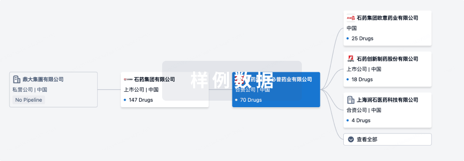
组织架构
使用我们的机构树数据加速您的研究。
登录
或
管线布局
2026年07月22日管线快照
管线布局中药物为当前组织机构及其子机构作为药物机构进行统计,早期临床1期并入临床1期,临床1/2期并入临床2期,临床2/3期并入临床3期
其他
1
登录后查看更多信息
当前项目
| 药物(靶点) | 适应症 | 全球最高研发状态 |
|---|---|---|
FLX-787 ( TRPA1 x TRPV1 ) | 多发性硬化症 更多 | 终止 |
登录后查看更多信息
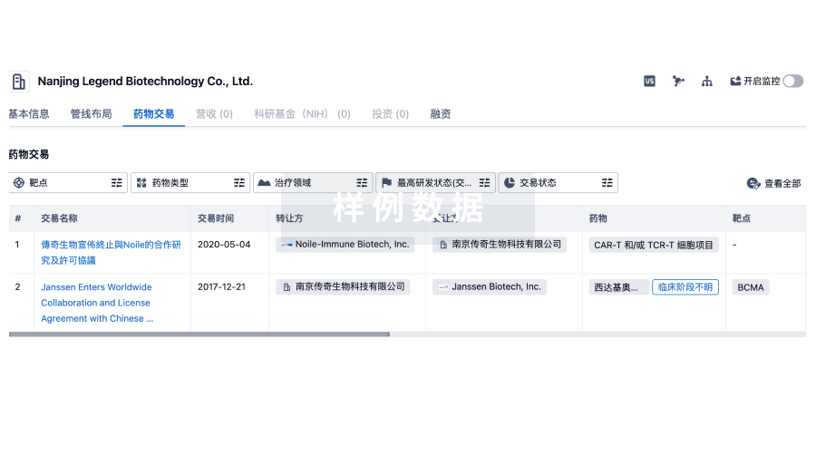
药物交易
使用我们的药物交易数据加速您的研究。
登录
或
转化医学
使用我们的转化医学数据加速您的研究。
登录
或
营收
使用 Synapse 探索超过 36 万个组织的财务状况。
登录
或
科研基金(NIH)
访问超过 200 万项资助和基金信息,以提升您的研究之旅。
登录
或
投资
深入了解从初创企业到成熟企业的最新公司投资动态。
登录
或
融资
发掘融资趋势以验证和推进您的投资机会。
登录
或
芽仔
全新生物医药AI Agent 覆盖科研全链路,让突破性发现快人一步
立即开始免费试用!
智慧芽新药情报库是智慧芽专为生命科学人士构建的基于AI的创新药情报平台,助您全方位提升您的研发与决策效率。
立即开始数据试用!
智慧芽新药库数据也通过智慧芽数据服务平台,以API或者数据包形式对外开放,助您更加充分利用智慧芽新药情报信息。
生物序列数据库
生物药研发创新
免费使用
化学结构数据库
小分子化药研发创新
免费使用