预约演示
更新于:2026-03-05
The University of Tokushima
更新于:2026-03-05
概览
标签
其他疾病
口颌疾病
心血管疾病
重组多肽
小分子化药
化学药
疾病领域得分
一眼洞穿机构专注的疾病领域
暂无数据
技术平台
公司药物应用最多的技术
暂无数据
靶点
公司最常开发的靶点
暂无数据
| 排名前五的药物类型 | 数量 |
|---|---|
| 重组多肽 | 2 |
| 小分子化药 | 1 |
| 化学药 | 1 |
| 中药 | 1 |
| 间充质干细胞疗法 | 1 |
| 排名前五的靶点 | 数量 |
|---|---|
| TNF-α(肿瘤坏死因子α) | 1 |
| NHE5(钠氢交换蛋白-5) | 1 |
关联
6
项与 The University of Tokushima 相关的药物靶点 |
作用机制 TNF-α抑制剂 |
非在研适应症 |
最高研发阶段批准上市 |
首次获批国家/地区 日本 |
首次获批日期1957-08-21 |
靶点- |
作用机制- |
在研适应症 |
非在研适应症- |
最高研发阶段临床前 |
首次获批国家/地区- |
首次获批日期- |
靶点 |
作用机制 NHE5抑制剂 |
在研适应症 |
非在研适应症- |
最高研发阶段临床前 |
首次获批国家/地区- |
首次获批日期- |
144
项与 The University of Tokushima 相关的临床试验JPRN-UMIN000054536
Investigation of the Efficacy of Pain Relief Using Sucrose and Pacifier in Fundus Examination - Investigation of the Efficacy of Pain Relief Using Sucrose and Pacifier in Fundus Examination
开始日期2024-07-01 |
申办/合作机构 |
JPRN-UMIN000054244
Preimplantaion testing for monogenic disease(congenital myopathy) - Preimplantation testing for monogenic disease(congenital myopathy)
开始日期2024-06-01 |
申办/合作机构 |
JPRN-UMIN000053260
Optimizing flow rate of high-flow nasal cannula using peak inspiratory flow during spontaneous breathing trial for post-extubation pediatric populations - Optimizing flow rate of high-flow nasal cannula using peak inspiratory flow during spontaneous breathing trial for post-extubation pediatric populations
开始日期2024-02-01 |
申办/合作机构 |
100 项与 The University of Tokushima 相关的临床结果
登录后查看更多信息
0 项与 The University of Tokushima 相关的专利(医药)
登录后查看更多信息
5,198
项与 The University of Tokushima 相关的文献(医药)2025-11-01·DIFFERENTIATION
Osteocyte-like differentiation of osteosarcoma by inorganic phosphate
Article
作者: Katayama, Ryohei ; Koike, Sumie ; Suzuki, Yuya ; Takagi, Satoshi ; Takeuchi, Makoto
Osteosarcoma (OS) cells that deviate from the normal osteogenic differentiation pathway from mesenchymal stem cells (MSCs) to less migratory osteocytes are in an undifferentiated and highly malignant state. β-glycerophosphate (β-gp) is commonly used to induce the osteogenic differentiation of MSCs, inorganic phosphate (Pi) is also widely used to promote MSC differentiation into osteocytes. Recently, OS cells were found to differentiate into an osteocyte-like state by culturing in osteocyte differentiation medium containing β-gp, dexamethasone, and ascorbate. However, whether Pi can induce the osteogenic differentiation of OS cells and its underlying mechanisms remain unclear. In this study, we evaluated the ability of two types of Pi (i.e., disodium phosphate [Na2HPO4] and monosodium phosphate [NaH2PO4]) to promote the osteogenic differentiation of OS cells. Culturing OS cells in Pi-supplemented medium resulted in increased osteogenic marker gene expression and calcium deposition and reduced cell motility. Notably, Na2HPO4 exhibited particularly strong differentiation-inducing effects. Furthermore, our data suggest that WNT5b, a key factor of the noncanonical Wnt signaling pathway, is involved in the Na2HPO4-induced osteogenic differentiation of OS cells. These findings suggest that above 3 mM of Na2HPO4 function as an inducer of osteocyte-like differentiation in OS cells and that targeting this pathway may offer new therapeutic strategies to suppress OS metastasis.
2025-03-01·SYNLETT
Synthesis of Methyl 2-[Bis(benzylthio)phosphoryl]acetate as a Novel Horner–Wadsworth–Emmons-Type Reagent and Its Application to the Diastereodivergent Synthesis of (E)- and (Z)-α,β-Unsaturated Esters
作者: Seki, Kazumasa ; Nakao, Michiyasu ; Yamada, Shoki ; Ihara, Takahito ; Kitaike, Syuji ; Sano, Shigeki
Abstract:
Methyl 2-[bis(benzylthio)phosphoryl]acetate has proven to be an efficient Horner–Wadsworth–Emmons (HWE)-type reagent for the diastereodivergent synthesis of (E)- and (Z)-α,β-unsaturated esters. Under the conditions of excess NaHMDS relative to the HWE-type reagent, the HWE-type reactions of methyl 2-[bis(benzylthio)phosphoryl]acetate with various aldehydes afforded the corresponding α,β-unsaturated esters in an E-selective manner in up to 100:0 E/Z ratio. However, when an excess of the HWE-type reagent was used relative to NaHMDS, the stereoselectivity of the HWE-type reactions was dramatically changed from E to Z, yielding an E/Z ratio of up to 2:98.
2025-02-10·MODERN PHYSICS LETTERS B
Laser ablation synthesis of BiOCl/Ag/WO3 nanocomposite to evaluate its photocatalysis performance
作者: Katayama, Testuro ; Furube, Akihiro ; Koinkar, Pankaj ; Lin, Kai-Siang ; Wu, Chang Mou
Bismuth oxychloride (BiOCl)/silver (Ag)/tungsten oxide (WO3) nanocomposite was produced by laser ablation to enhance photocatalytic performance. The ternary nanocomposite showed a superior photocatalytic activity for methylene blue (MB) degradation under visible light compared to pure BiOCl and BiOCl/Ag with degradation up to 74%, 62%, and 52 %, respectively. The addition of Ag improved the dispersibility of BiOCl and WO3, which reduced the recombination of electron–hole pairs and can be responsible for higher photocatalytic activity.
3
项与 The University of Tokushima 相关的新闻(医药)2024-01-26
For Print(224KB) January 26, 2024
Eisai Co., Ltd. (Headquarters: Tokyo, CEO: Haruo Naito, “Eisai”) announced today that it has submitted a New Drug Application (NDA) for ultrahigh-dose mecobalamin (development code: E0302) for the indication of amyotrophic lateral sclerosis (ALS) to the Pharmaceuticals and Medical Devices Agency (PDMA) in Japan. In May 2022, ultrahigh-dose mecobalamin received orphan drug designation by the Ministry of Health, Labour and Welfare (MHLW).
This application is based on the results of JETALS (The Japan Early-Stage Trial of Ultrahigh-Dose Methylcobalamin for ALS), a Phase III trial to evaluate efficacy and safety of ultrahigh-dose methylcobalamin (mecobalamin) in early onset ALS patients, that was conducted as an investigator-initiated trial by a research team with Extraordinary Professor Ryuji Kaji (Principal Investigator), Tokushima University, and Professor Yuishin Izumi (Coordinating Investigator), the Department of Neurology, Tokushima University Graduate School of Biomedical Sciences, and Professor Satoshi Kuwabara (Coordinating Investigator), the Department of Neurology, Chiba University Graduate School of Medicine. The results of JETALS were published in the peer-reviewed journal JAMA Neurology.
ALS is an intractable, progressive, neurodegenerative disease that results in severe muscle atrophy and weakness in the muscles due to motor neuron dysfunction. As the main cause of death is respiratory failure due to paralysis of the respiratory muscles, without the use of an artificial respirator, death occurs within approximately 3 to 6 years from the onset of the disease. The number of patients in Japan is estimated to be approximately 10,000. Currently, there is no curative treatment established for ALS, and since there are only limited number of medicines approved in Japan and abroad, this is a disease with significant unmet medical needs.
Eisai considers neurology a therapeutic area of focus. As a human healthcare company, Eisai is committed to fulfill unmet medical needs in neurology and further its contribution to improving the benefit of patients and the people in the daily living domain.
Media Inquiries:
Public Relations Department,
Eisai Co., Ltd.
+81-(0)3-3817-5120
[Notes to editors]
Mecobalamin (generic name, development code: E0302) is approved and marketed as Methycobal®, a 500 µg injection of mecobalamin indicated for the treatment of peripheral neuropathies and megaloblastic anemia caused by vitamin B12 deficiency. Methycobal is also approved as a tablet formulation (250µg and 500 µg) as well as a fine granule formulation (0.1%) indicated for the treatment of peripheral neuropathies. While the mechanism of action of mecobalamin in amyotrophic lateral sclerosis (ALS) is not known, it has been suggested in non-clinical research that mecobalamin may have efficacy through a neuroprotective effect and regeneration of nerve axons. Since the 1990s, clinical research has been carried out on ultrahigh-dose mecobalamin in ALS by a study group on neurodegenerative disease, funded through the Ministry of Health, Labour and Welfare's Specified Disease Treatment Research Program. Short- and long-term trials of intramuscular injection of mecobalamin at 25 mg and 50 mg per day, which is respectively 50 and 100 times the approved dosage of Methycobal, suggested that ultrahigh-dose mecobalamin could have a clinical effect in ALS. Therefore, Eisai had conducted the Phase II/III clinical trial (Study 761) since 2006 and submitted a new drug application for ultrahigh-dose mecobalamin as treatment for ALS in May 2015 but withdrew the application in March 2016 after the Pharmaceuticals and Medical Devices Agency (PMDA) indicated that additional clinical trials were necessary.
Following favorable clinical trial results in JETALS, Eisai prepared to file a new drug application for ALS in Japan.
Full text(224KB)
临床3期申请上市孤儿药上市批准
2022-07-16
Optical nano-imaging techniques find immense applications in nanotechnology for visualizing nanoscale defects in samples. However, it is challenging to image large micron-sized samples at nanoscale resolution owing to signal distortions resulting from unavoidable thermal and mechanical drifts of the system over time. Now, researchers from Japan have developed an ultrastable nano-imaging system that successfully detects unique nanoscale defects not observed in conventional nano-imaging in micron-scale tungsten disulfide samples, widening the technique's scope to biological samples.
Raman spectroscopy, an optical microscopy technique, is a non-destructive chemical analysis technique that provides rich molecular fingerprint information about chemical structure, phase, crystallinity, and molecular interactions. The technique relies on the interaction of light with chemical bonds within a material. However, since light is a wave, optical microscopes are unable to resolve distances less than half the wavelength of the light incident on the sample. This is known as the "diffraction limit," which prevents Raman spectroscopy and other optical microscopy techniques from reaching nanoscale resolutions.
To improve the spatial resolution, another technique called "tip-enhanced Raman spectroscopy" (TERS) was invented, which can reach spatial resolutions below the diffraction limit. In TERS, a metallic nano-sized tip confines the light within a nano-sized volume just above the sample. The light interacts with the sample molecules on the surface and the imaging is performed by analyzing the scattered light.
TERS has been successfully used to analyze chemical compositions and surface defects in sample at nanoscale resolutions. However, during imaging, the nanotip tends to drift due to unavoidable thermal and vibrational fluctuations under ambient conditions, causing either the sample to be out-of-focus or misalignment between the nanotip and focal spot, or both. This causes considerable distortions in the scattered signals. To avoid this, TERS imaging needs to be completed within a time window of 30 minutes, a restriction that prevents imaging of any sample larger than 1 µm2 with nanoscale resolution.
In a new study published in Science Advances, a research team from Japan, led by Dr. Ryo Kato, a designated Assistant Professor at the Institute of Post-LED Photonics at Tokushima University, and Associate Professor Takayuki Umakoshi and Professor Prabhat Verma from Osaka University, has now developed, for the first time, a stable TERS system that is not limited to a short imaging time window. The team demonstrated its capability by successfully imaging nanoscale defects over a period of 6 hours in a micrometer-sized, two-dimensional (2D) tungsten disulfide (WS2) film -- a material commonly used in optoelectronic devices. "Our new optical nano-imaging system enables characterization of defect analysis in large-sized WS2 layers at a high pixel resolution down to 10 nm without any significant loss of optical signal," says Dr. Kato.
To compensate for the drifts over extended periods, the team developed a feedback system that tracks the displacement of the focused light source and readjusts the position of the focus plane accordingly. The focal position of the light source is tracked by measuring the displacement of a reflected laser guide beam directed into the microscope. The focus is then stabilized with a piezo-controlled objective scanner whenever the system senses a drift or a change in the focal position of the light source.
To stabilize the nanotip, the team designed a laser-scanning-assisted tip drift compensation system. In this case, galvano-scanners take images of the laser spot around the metallic nanotip just as it approaches the sample surface. This image appears as a bright spot and indicates the position of the nanotip. Once the measurement at a particular pixel has been carried out, the image of the laser spot around the nanotip is captured again. The laser spot is then moved to match the new position of the nanotip in this image. The process continues throughout the imaging process, ensuring the nanotip remains at a constant position.
By implementing these corrections, the team was able to image a 2D sheet of WS2 with a scan area of 1 × 4 µm2. With a 12 times longer imaging time window than that of conventional imaging, they could detect unique defects missed in conventional TER imaging. They also showed that the defect density on a larger WS2 sample (comparable to device scales) was higher than that reported for smaller samples.
The study could open doors to precise, high-resolution imaging of not only optoelectronic devices but also biological samples. "Our new drift-compensated TERS microscopy could not only evaluate surface properties of device materials better but also allow us to study biological processes such as the mechanism underlying the development of diseases. This, in turn, could help develop novel clinical methods and therapies," speculates Dr. Umakoshi. These are certainly some exciting possibilities to contemplate!
2021-01-06
A new fluorescence lifetime microscopy breakthrough led by scientists from Tokushima University holds potential in several areas within life sciences
The recent breakthrough was achieved by simultaneously mapping 44,400 "light stopwatches" to measure fluorescence lifetime (Credit: Tokushima University)
Scientists have developed a new microscopy technique that harnesses the lifetime of fluorescence, as well as its intensity, to capture more comprehensive images.
The breakthrough, which was made by a team from Tokushima University, Japan, is likely to be “helpful” in life sciences, where dynamic observations of living cells and chemical processes are key.
As well as holding promise in the development of novel therapeutic options, this new approach could also be used for simultaneous imaging of multiple samples in antigen testing – which is currently being deployed widely to diagnose Covid-19.
Conventional microscopy with fluorescence – the absorption and re-emission of light by molecules – provides poor quantitative information on samples because it only captures intensity of the light emitted, which changes frequently and depends on external factors.
But, using light sources known as frequency combs, a team from Tokushima University in Japan has developed a way of measuring both fluorescence intensity and lifetime, and producing images from all points in the sample simultaneously, without the need for mechanical parts.
Professor Takeshi Yasui from the Institute of Post-LED Photonics (pLED) at Tokushima University, who led the study, said: “Our method can be interpreted as simultaneously mapping 44,400 light stopwatches over a 2D space to measure fluorescence lifetimes – all in a single shot, and without scanning.
“Because our technique does not require scanning, a simultaneous measurement over the entire sample is guaranteed in each shot.
“This will be helpful in life sciences, where dynamic observations of living cells are needed.”
Challenges in fluorescence lifetime microscopy
Fluorescence microscopy is widely used in the biochemistry and life sciences sectors as it allows scientists to directly observe cells, and certain compounds in and around them.
However, the major limitation of conventional fluorescence microscopy techniques is that the results they produce are difficult to evaluate quantitatively, because fluorescence intensity is significantly affected by experimental conditions and the concentration of the fluorescent substance.
One way around this is to focus on fluorescence lifetime instead of intensity, as this factor is independent of experimental conditions.
When a fluorescent substance is irradiated with a short burst of light, the re-emitted light does not disappear immediately but ‘decays’ over time in a way that is specific to the substance in question.
However, fluorescence lifetime microscopy – a technique that leverages this phenomenon, and is able to accurately quantify fluorescent molecules and changes in their environment – presents its own difficulties.
The decay of fluorescence is extremely fast, and the single-point photodetectors that are traditionally used involve the movement of mechanical pieces, greatly limiting the speed of the image capturing.
How did scientists develop a new technique to overcome these difficulties?
In a recent study published in online scientific journal Science Advances, the team from Tokushima University outlined how they developed a novel approach for acquiring fluorescence lifetime images without the need for mechanical scanning.
One of the main pillars of the method they used is an optical frequency comb – which is essentially a light signal composed of many discrete, evenly-spaced optical frequencies that resembles a hair comb when plotted against optical frequency.
Using special optical equipment, a pair of excitation frequency comb signals are decomposed into individual optical beat signals with different intensity-modulation frequencies, each carrying a single modulation frequency, and irradiated on the target sample.
The key here is that each light beam hits the sample on a spatially-distinct location, creating a one-to-one correspondence between each point on the 2D surface of the sample and each modulation frequency of the optical beats.
Because of its fluorescent properties, the sample re-emits part of the captured radiation while still preserving the aforementioned frequency-position correspondence.
The fluorescence emitted from the sample is then simply focused using a lens onto a high-speed single-point photodetector, which – thanks to this method’s superior speed and high spatial resolution – produces an image that takes into account fluorescence lifetime measurements.
100 项与 The University of Tokushima 相关的药物交易
登录后查看更多信息
100 项与 The University of Tokushima 相关的转化医学
登录后查看更多信息
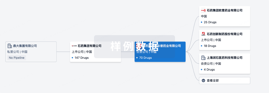
组织架构
使用我们的机构树数据加速您的研究。
登录
或
管线布局
2026年05月02日管线快照
管线布局中药物为当前组织机构及其子机构作为药物机构进行统计,早期临床1期并入临床1期,临床1/2期并入临床2期,临床2/3期并入临床3期
临床前
6
6
其他
登录后查看更多信息
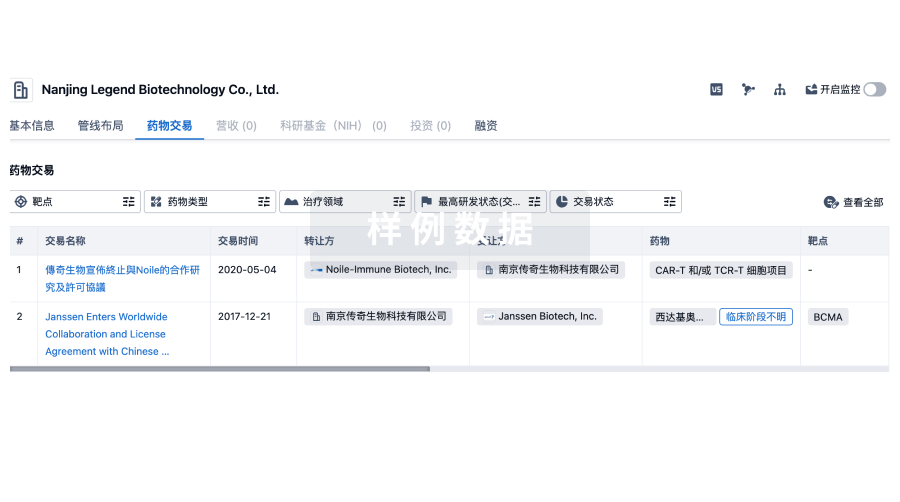
药物交易
使用我们的药物交易数据加速您的研究。
登录
或
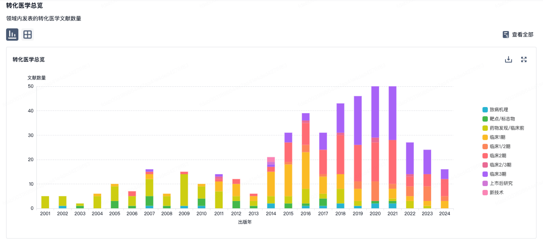
转化医学
使用我们的转化医学数据加速您的研究。
登录
或
营收
使用 Synapse 探索超过 36 万个组织的财务状况。
登录
或

科研基金(NIH)
访问超过 200 万项资助和基金信息,以提升您的研究之旅。
登录
或
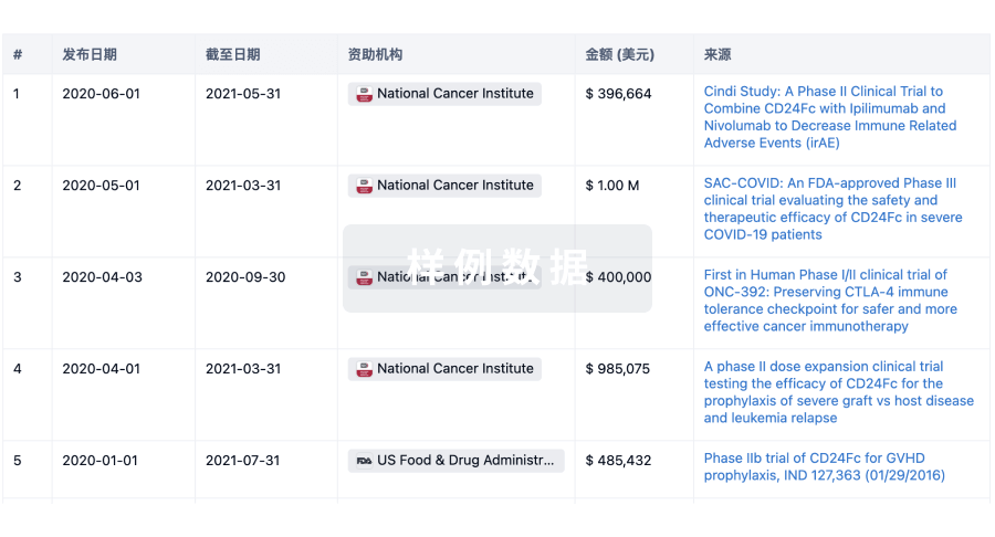
投资
深入了解从初创企业到成熟企业的最新公司投资动态。
登录
或
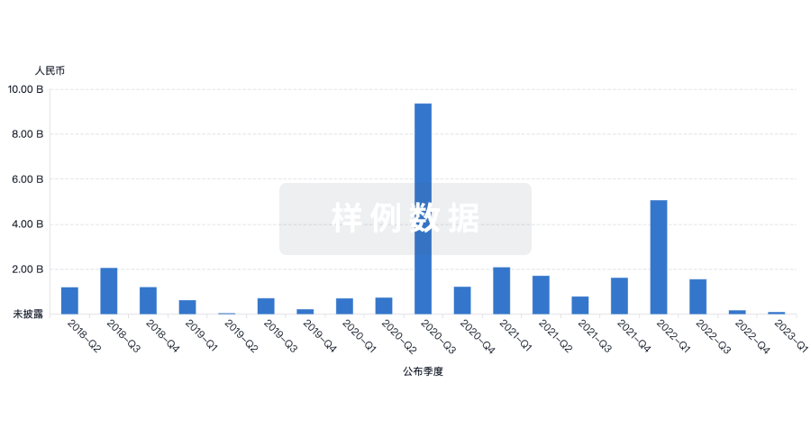
融资
发掘融资趋势以验证和推进您的投资机会。
登录
或
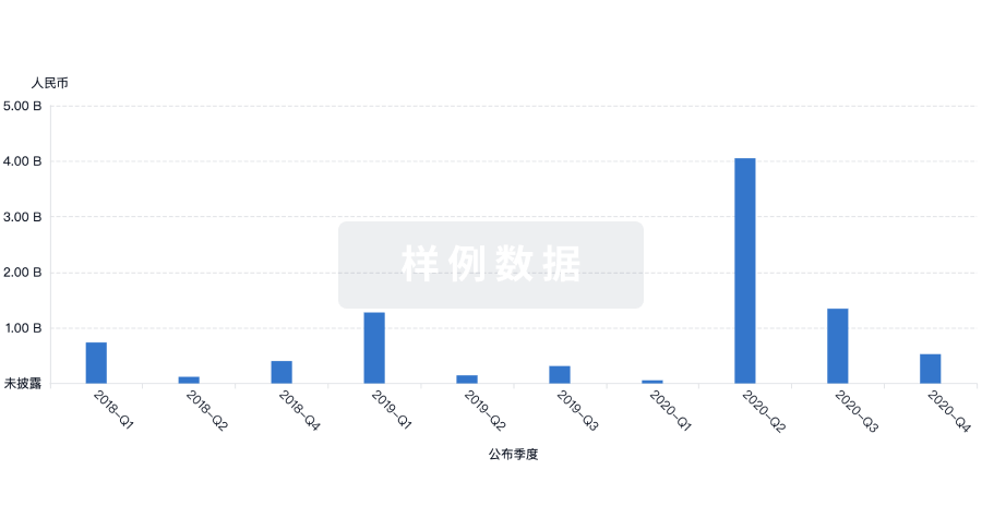
生物医药百科问答
全新生物医药AI Agent 覆盖科研全链路,让突破性发现快人一步
立即开始免费试用!
智慧芽新药情报库是智慧芽专为生命科学人士构建的基于AI的创新药情报平台,助您全方位提升您的研发与决策效率。
立即开始数据试用!
智慧芽新药库数据也通过智慧芽数据服务平台,以API或者数据包形式对外开放,助您更加充分利用智慧芽新药情报信息。
生物序列数据库
生物药研发创新
免费使用
化学结构数据库
小分子化药研发创新
免费使用