预约演示
更新于:2025-12-17

Kyushu University
更新于:2025-12-17
概览
标签
肿瘤
其他疾病
心血管疾病
小分子化药
基因疗法
ASO
疾病领域得分
一眼洞穿机构专注的疾病领域
暂无数据
技术平台
公司药物应用最多的技术
暂无数据
靶点
公司最常开发的靶点
暂无数据
| 排名前五的药物类型 | 数量 |
|---|---|
| 小分子化药 | 11 |
| 基因疗法 | 2 |
| 化学药 | 1 |
| ASO | 1 |
| 合成肽疫苗 | 1 |
关联
16
项与 Kyushu University 相关的药物作用机制 P2X7 receptor拮抗剂 |
非在研适应症- |
最高研发阶段批准上市 |
首次获批国家/地区 美国 |
首次获批日期2019-12-20 |
靶点 |
作用机制 CCL2抑制剂 |
非在研适应症- |
最高研发阶段批准上市 |
首次获批国家/地区 日本 |
首次获批日期1994-07-01 |
靶点 |
作用机制 FGF2基因转移 [+1] |
最高研发阶段临床2期 |
首次获批国家/地区- |
首次获批日期- |
177
项与 Kyushu University 相关的临床试验NCT06983210
Multi-center, Open-Label, Single Arm Trial for Evaluation of the Efficacy and Safety in the First Line Combination Therapy of Gemcitabine, Cisplatin and Nivolumab With Additional Pretreatment of AM80 for Urothelial Carcinoma Patients
【Treatment of Urothelial Carcinoma】 Treatment for urothelial carcinoma includes surgery, chemotherapy (anticancer drugs), and radiation therapy. Chemotherapy is generally used when metastasis has already occurred at diagnosis and surgery is not curative (metastatic urothelial carcinoma) or when the cancer recurs after local therapy such as surgery or radiation therapy (recurrent urothelial carcinoma).
Although there are several recommended treatments for urothelial carcinoma, the options are often limited by side effects and other factors, and these treatments may not be fully effective. Therefore, the development of safer and more effective treatments is desired.
【About the Drugs to be Used in this Clinical Trial】 In this clinical trial, the investigational drug MIKE-1 will be used in combination with nivolumab plus GC (cisplatin gemcitabine), one of the recommended chemotherapy regimens, and subsequently with nivolumab monotherapy for patients with unresectable metastatic or recurrent urothelial cancer. Nivolumab, cisplatin, and gemcitabine are injectable (intravenous infusion), while MIKE-1 is oral.
【Purpose of the Clinical Trial】 The purpose of this clinical trial is to evaluate the efficacy (how much the cancer shrinks or slows down) and safety of the investigational drug MIKE-1 in combination with nivolumab and gemcitabine and cisplatin therapy in patients with untreated unresectable or recurrent urothelial cancer.
开始日期2025-05-01 |
申办/合作机构  Nagoya University Nagoya University [+5] |
JPRN-UMIN000054209
Development of feedback strategies for behavior modification through the use of healthcare databases - Development of feedback strategies for behavior modification through the use of healthcare databases
开始日期2024-06-01 |
申办/合作机构 |
JPRN-UMIN000054913
Establishment of a Multiparameter Flow Cytometry (MFC) Method for Measuring Minimal Residual Disease in Acute Myeloid Leukemia - Establishment of MFC Method for Measuring MRD in AML
开始日期2024-05-23 |
申办/合作机构 |
100 项与 Kyushu University 相关的临床结果
登录后查看更多信息
0 项与 Kyushu University 相关的专利(医药)
登录后查看更多信息
78,808
项与 Kyushu University 相关的文献(医药)2026-03-01·NURSE EDUCATION TODAY
Effectiveness of 360-degree video materials for enhancing emotional readiness and spatial comprehension in nursing students during operating room practicum: A prospective controlled study
Article
作者: Nakata, Kohei ; Hisada, Yukiko ; Kinoshita, Yumiko ; Moriyama, Tomohiko ; Kudo, Kuriko ; Nagayoshi, Kinuko ; Nakamura, Masafumi ; Kanaoka, Maki ; Matsuoka, Mie ; Nakamura, Misato ; Izukura, Rieko
BACKGROUND:
Operating room (OR) practice often induces anxiety in nursing students because of its highly specialized environment. Innovative preparatory education is essential to enhance students' emotional readiness and spatial understanding prior to clinical exposure. This study aimed to evaluate the effectiveness of 360-degree video materials in improving emotional and spatial preparedness among nursing students before and after an OR practicum.
METHODS:
This study was conducted in a single nursing school in Japan and included 61 third-year nursing students undergoing OR practicums between September 2024 and January 2025. Students were sequentially assigned to a 360-degree video group (n = 22) or a control group (n = 25). Emotional responses (interest, enjoyment, excitement, fear, and anxiety), OR practicum-related stress, and spatial comprehension (patient flow, nurse workflow, and equipment layout) were assessed before the practicum, after video viewing, and after the practicum.
RESULTS:
No significant differences were observed between the groups at baseline. After viewing the 360-degree video, the proportion of students who reported interest, enjoyment, and excitement increased significantly. These positive emotional responses were enhanced after the practicum. The proportion of students who reported anxiety (before the practicum: 68.1 %; after viewing: 50.0 %; after the practicum: 22.7 %; P = 0.002) significantly decreased following exposure to the video and continued to decrease after the practicum. Empathy toward patients improved progressively (before the practicum: 77.3 %; after viewing: 90.0 %: after the practicum: 100.0 %; P = 0.04). Spatial comprehension improved significantly after video exposure and continued to increase after the practicum.
CONCLUSIONS:
Integrating 360-degree video into preparatory education effectively enhanced nursing students' emotional readiness and spatial understanding of OR practicums. This approach may contribute to reducing pre-practicum anxiety and facilitate deeper engagement in clinical education.
2026-02-01·JOURNAL OF COLLOID AND INTERFACE SCIENCE
Tailoring water freezing kinetics with nanobubbles: A gas-dependent modulatory effect on water solidification
Article
作者: Yamamoto, Natsuki ; Kioka, Arata
HYPOTHESIS:
This study hypothesised that nanobubbles (NBs) can significantly influence the time required for water to undergo a complete liquid-to-solid phase transition (solidification). We further posited that this effect is dependent on the gas species used to generate the NBs, driven by their unique interfacial electrical properties and impact on ice nucleation and the water liquid-solid interface in water solidification.
EXPERIMENTS AND SIMULATIONS:
Laboratory experiments were conducted to investigate the effect of air NBs and CO2 NBs on water solidification time. The experiments measured the time to complete water solidification at ambient temperatures of -10 °C and - 20 °C. Concurrently, numerical simulations of transient heat conduction were performed to assess the apparent energy released during the phase transition in the presence of NBs, providing a comparative measure for the observed solidification time changes.
FINDINGS:
The experimental results revealed that NBs do indeed alter the completion time of water solidification. Specifically, air NBs delayed solidification by up to 8.7 ± 1.9 %, while CO2 NBs accelerated it by up to 11.4 ± 2.5 % at an ambient temperature of -20 °C. This alteration can be explained by numerous OH- ions and the Hofmeister-like behaviour of CO32-. The numerical simulations corroborated these findings, showing that the observed changes in solidification time are comparable to an increase of +8 ± 2 % in the overall apparent energy released for air NBs and a decrease of -10 ± 2 % for CO2 NBs. These findings suggest that NBs, depending on the gas species, offer a promising "green" nanomaterial for controlling water freezing and anti-freezing processes.
2026-02-01·COMPARATIVE BIOCHEMISTRY AND PHYSIOLOGY C-TOXICOLOGY & PHARMACOLOGY
Ancestral exposure to amitriptyline disrupts the behavior and gene expression in zebrafish F2 offspring
Article
作者: Chen, Kun ; Takai, Yuki ; Qiu, Xuchun ; Oshima, Yuji ; Liu, Anqi ; Shimasaki, Yohei
Amitriptyline (AMI), a commonly used tricyclic antidepressant, has been identified as a significant pharmaceutical contaminant in aquatic environments. Although parental exposure of zebrafish to AMI has been found to induce changes in the development, behavior, and gene expression of their F1 offspring, it is unclear whether such adverse effects will be further extended to subsequent generations. In the current study, we explored the effects of ancestral exposure to AMI at environmentally relevant concentrations (0 and 0.8 μg/L) on the early life stages of zebrafish F2 offspring. The results showed that ancestral exposure to AMI had no significant effect on the survival and development of the zebrafish F2 offspring. However, significant hyperactivity was observed in the F2 larvae in the ancestral AMI exposure group during the dark periods of a light-dark locomotion assay. Transcription analysis revealed that ancestral exposure to AMI significantly disrupted pathways associated with xenobiotic biodegradation and metabolism, as well as the metabolism of cofactors and vitamins. Furthermore, ancestral exposure to AMI significantly decreased the level of cytochrome P450 and the activity of glutathione S-transferase within the F2 larvae, which are critical enzymes involved in xenobiotic metabolism. These findings provide valuable insights into the multigenerational effects of AMI exposure in zebrafish, emphasizing the importance of assessing the risks posed by such pollutants to fish populations.
37
项与 Kyushu University 相关的新闻(医药)2025-03-03
RSS
Otsuka Pharmaceutical Co., Ltd. (Otsuka) announces that the hematological tumor gene panel test HemeSite®, the first-in-Japan, comprehensive genomic profiling assay for hematological malignancies, is covered by Japan's national health insurance system, effective March 1. Sales have commenced today.
In recent years, classification and diagnostic criteria for hematological malignancies from the World Health Organization (WHO), as well as clinical treatment guidelines from medical societies around the world, highlight the critical importance of medical treatment based on genome information, making this information essential for the latest medical treatment.
In Japan, the usefulness of genomic information for diagnosis, treatment selection, and prognosis prediction is described in the Japanese Society of Hematology Genome Guidelines*1.
Insurance coverage for the cancer gene panel test for solid tumors exists in Japan, but until now insurance reimbursement has not been provided to any gene panel test for hematological malignancies.
HemeSight was developed jointly by Otsuka and the National Cancer Center Japan. Its performance has been verified by a research consortium*2 comprising the National Cancer Center, Kyushu University, Kyoto University, Nagoya Medical Center, the Institute of Medical Science at the University of Tokyo, and Keio University School of Medicine.
In hematological malignancies, genomic information is useful for treatment selection and for diagnosis and prognosis prediction, therefore the use of gene panel testing at the time of initial diagnosis is recommended in the Genome Medicine Promotion Act. From now on, the initial diagnosis of leukemia such as acute myeloid leukemia, malignant lymphoma, and multiple myeloma is covered by insurance. Accordingly, in the case of acute myeloid leukemia, HemeSight can be used for prognosis prediction based on genetic abnormalities and in the case of malignant lymphoma and multiple myeloma, it can be used for diagnosis when conventional methods cannot be used or when it is difficult to distinguish from other diseases.
In addition, diseases such as acute myeloid leukemia and Philadelphia chromosome-positive acute lymphoblastic leukemia are also covered by insurance when they recur or are refractory. Also, the start of insurance coverage may be beneficial to patients with unexplained, significant decreases in blood cells, for whom it has been difficult to determine treatment plans because definitive diagnoses could not be made.
The launch of the hematological tumor gene panel test HemeSight is expected to advance the social implementation of personalized medicine for hematological tumors in Japan.
Product Overview
The hematological tumor gene panel test HemeSight is composed of the in vitro diagnostic drug HemeSight Diagnostic Drug and the medical device program HemeSight Analysis Program.
*1 Japanese Society of Hematology Guidelines for Genomic Testing of Hematological Malignancies, 2021 Partially Revised Edition (http://www.jshem.or.jp/genomgl/home.html)
*2 Consists of an in vitro diagnostic product for hematological malignancies gene panel testing and its program.
基因疗法临床研究
2025-02-24
Researchers have uncovered a surprising layer of complexity in aldosterone-producing adenomas -- adrenal gland tumors that drive high blood pressure. Using cutting-edge analysis techniques, they discovered that these tumors harbor at least four distinct cell types, including ones that produce cortisol, the body's main stress hormone. Their findings not only explain why some patients with these tumors develop unexpected health issues, like weakened bones, but also pave the way toward new treatment strategies.
Kyushu University researchers have uncovered a surprising layer of complexity in aldosterone-producing adenomas (APAs) -- adrenal gland tumors that drive high blood pressure. Using cutting-edge analysis techniques, they discovered that these tumors harbor at least four distinct cell types, including ones that produce cortisol, the body's main stress hormone. Published in the week beginning 24 February in PNAS, their findings not only explain why some patients with APAs develop unexpected health issues, like weakened bones, but also pave the way toward new treatment strategies.
"Currently, the only way to cure APAs is through surgery to remove the tumor, and this hasn't changed for decades," says first author of the study, Assistant Professor Maki Yokomoto-Umakoshi, from the Department of Endocrine and Metabolic Diseases at Kyushu University Hospital. "To develop new treatment models, such as drug treatments, we urgently need to understand how these tumors work at the molecular level, and how the different cell types interact with each other."
APAs are benign (non-cancerous) tumors that develop on the adrenal glands -- small glands on top of the kidneys that produce important hormones, such as aldosterone, cortisol and sex hormones. Due to their location, APAs are a major cause of primary aldosteronism, a condition in which excessive production of the hormone aldosterone leads to high blood pressure. Primary aldosteronism is responsible for about 5-10% of high blood pressure cases, and patients with APAs have a higher risk of heart and blood vessel problems compared to people with common high blood pressure.
"Without proper treatment, patients can develop serious health problems like heart disease, diabetes, and bone weakness," adds Yokomoto-Umakoshi.
In this study, the researchers focused on APAs caused by changes in a gene called KCNJ5. This mutation, which accounts for around 40-70% of all cases of these tumors, is typically associated with larger tumors that form at a younger age, as well as more severe symptoms that cannot simply be explained by overproduction of aldosterone. However, the cellular makeup of KCNJ5 tumors, as well as which other hormones the tumors might secrete, has previously proven difficult to study.
To gain a deeper understanding of APAs, the research team, led by Professor Yoshihiro Ogawa from Kyushu University and in collaboration with Osaka University, Kyoto University, and the University of Tokyo, applied a combination of advanced techniques, providing the first comprehensive view of APAs in unprecedented detail. The researchers were able to map where different cell types were located within these tumors, and how they work together. Furthermore, the techniques allowed the researchers to reveal diverse genetic variation within different regions of APAs and identify exactly which hormones the tumors were producing.
The study revealed that APAs are more complex than previously thought, consisting of at least four distinct cell types. The tumor starts with cells that respond to stress, which can then develop into either cells that make aldosterone, or cells that make cortisol. The cortisol-producing cells can then further develop into stromal-like cells that help the tumor to grow.
The researchers also discovered that special immune cells called lipid-associated macrophages were more abundant within the tumor, with a potential role in influencing hormone production and tumor growth.
"Overall, these tumors contain diverse hormone-producing cells that can affect patient's health in different ways -- not just through high blood pressure, but also through other symptoms caused by excess cortisol, like bone weakness," explains Yokomoto-Umakoshi.
In the future, the researchers plan to use these techniques to extend their analysis to other types of APAs, as well as to other tumors that produce excess hormones. They also hope that their current findings help set the stage for developing future drug treatments for APAs.
"Now we understand more about APAs, it opens up promising new treatment strategies, such as directly targeting lipid-associated macrophages or excess cortisol," concludes Yokomoto-Umakoshi.
2024-09-30
RSS Share
Otsuka Pharmaceutical Co., Ltd. (Tokyo); The National Cancer Center Japan (Tokyo); Kyushu University (Fukuoka); Kyoto University (Kyoto); Nagoya Medical Center (Aichi); Advanced Clinical Research Center, The Institute of Medical Science at The University of Tokyo (Tokyo); and Keio University School of Medicine (Tokyo) announce today that Otsuka Pharmaceutical has received approval to manufacture and market HemeSight®, hematological malignancies gene panel test, in Japan. Otsuka will proceed on procedures to qualify HemeSight for health insurance reimbursement and will start marketing the test as soon as launch preparations are completed.
HemeSight was developed jointly by Otsuka Pharmaceutical and the National Cancer Center, and its performance has been verified by a research consortium*1 comprising the National Cancer Center, Kyushu University, Kyoto University, and the Nagoya Medical Center.
Insurance coverage for the cancer gene panel test for solid tumors already exists in Japan. However there was no approved gene panel test for hematological malignancies, and cancer genome medicine has not yet been covered by health insurance reimbursement.
This product is the first gene panel test for hematological malignancies and related diseases to be designated as a product subject to the "review system for designated world-first products" *2 by Japan's Ministry of Health, Labour and Welfare*3 and approved for manufacture and marketing in Japan. The product consists of the in vitro diagnostic product HemeSight In Vitro Diagnostics and the medical device program HemeSight Analysis Program.
In recent years, diagnosis and treatment guidelines for hematological malignancies proposed by the World Health Organization (WHO) and other organizations recommend medical treatment based on genome information, and it is becoming increasingly difficult to make an appropriate diagnosis and treatment without using genome information.
In Japan, the Japanese Society of Hematology has issued guidelines for genomic testing of hematological malignancies*4, which provide recommendations for gene panel testing for each disease and stage, including leukemia, malignant lymphoma, and multiple myeloma. HemeSight is designed to comprehensively test for the genetic abnormalities of hematological malignancies listed in the guidelines, and is expected to enable diagnosis, treatment selection, and prognosis prediction based on genetic abnormalities.
The approval of the hematological malignancies gene panel test HemeSight is expected to greatly advance personalized medicine in the field of hematopoietic oncology in Japan and contribute to better medical care.
Professor Koichi Akashi, Department of Pathology and Restorative Medicine, Graduate School of Medicine, Kyushu University, commented, "In recent years, cancer genome medicine has made rapid progress since the gene panel tests for solid tumors have become covered by insurance. A hematological malignancies genome test guideline was issued with the aim of implementing cancer genome medicine, but there was no gene panel test that could be used for hematological malignancies. With the approval of the hematological malignancies gene panel test, we hope that cancer genomic medicine will advance in hematological malignancies as well, enabling optimal treatment for each individual patient.
Tatsuaki Ohashi, general manager of the Diagnostics Division of Otsuka Pharmaceutical, said, "HemeSight is the first hematological malignancies gene panel test in Japan. We would like to thank all the medical professionals who participated in the joint research consortium and all the patients and stakeholders who were involved in its development. Otsuka Pharmaceutical has been manufacturing and marketing in vitro diagnostics for genetic testing for acute leukemia. With the enactment of the Genomic Medicine Promotion Act, we are very pleased to add HemeSight for hematological malignancies and related diseases to our new product lineup. Hematological malignancies are the most common pediatric cancer, and the number of adults with this disease is also increasing. We look forward to contributing to personalized medicine for all patients with hematological malignancies, both adult and pediatric, who need it."
Gretchen Weightman, Illumina's senior vice president, Asia-Pacific, Middle East & Africa, who also signed the development and commercialization agreement for this product*5 on behalf of Illumina, said: 'We are very pleased with the approval of HemeSight in Japan. As Otsuka Pharmaceutical's technology partner for genomic sequencing, we are proud to support Otsuka and healthcare organizations in providing comprehensive genomic profiling for patients with hematological malignancies."
*1. Consists of an in vitro diagnostic product for hematological malignancies gene panel testing and its program. *2. Development of the first comprehensive genomic profiling assay for hematologic malignancies in Japan (https://www.otsuka.co.jp/en/company/newsreleases/2020/20200326_2.html) *3. Act on Comprehensive and Systematic Promotion of Measures to Ensure that the Public is Securely Able to Receive High-Quality and Appropriate Genomic Medicine (Act No. 57 of 2023) *4. Japanese Society of Hematology Guidelines for Genomic Testing of Hematological Malignancies, 2021 Partially Revised Edition (http://www.jshem.or.jp/genomgl/home.html) *5. Otsuka and Illumina Announce Agreement on Development and Commercialization of IVD Test Kit for Patients in Japan with Blood Cancer (https://www.otsuka.co.jp/en/company/newsreleases/2021/20210203_1.html)
上市批准基因疗法
100 项与 Kyushu University 相关的药物交易
登录后查看更多信息
100 项与 Kyushu University 相关的转化医学
登录后查看更多信息
组织架构
使用我们的机构树数据加速您的研究。
登录
或
管线布局
2026年04月30日管线快照
管线布局中药物为当前组织机构及其子机构作为药物机构进行统计,早期临床1期并入临床1期,临床1/2期并入临床2期,临床2/3期并入临床3期
药物发现
2
10
临床前
临床1期
2
2
临床2期
其他
11
登录后查看更多信息
当前项目
| 药物(靶点) | 适应症 | 全球最高研发状态 |
|---|---|---|
成纤维细胞生长因子2基因疗法(Id Pharma Co., Ltd.) ( bFGF ) | 间歇性跛行 更多 | 临床2期 |
DVC1-0401 ( PEDF ) | 视网膜色素变性 更多 | 临床1/2期 |
NC-2600 ( P2X4 receptor ) | 神经痛 更多 | 临床1期 |
Tax peptide-pulsed dendritic cell vaccine(Tokyo Medical & Dental University) | T细胞淋巴瘤 更多 | 临床1期 |
亮蓝G ( P2X7 receptor ) | 视网膜变性 更多 | 临床前 |
登录后查看更多信息
药物交易
使用我们的药物交易数据加速您的研究。
登录
或
转化医学
使用我们的转化医学数据加速您的研究。
登录
或
营收
使用 Synapse 探索超过 36 万个组织的财务状况。
登录
或
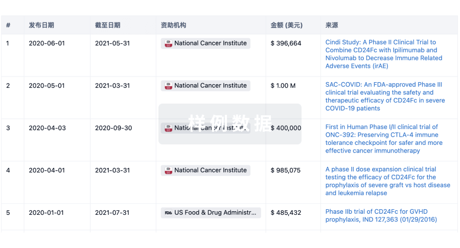
科研基金(NIH)
访问超过 200 万项资助和基金信息,以提升您的研究之旅。
登录
或
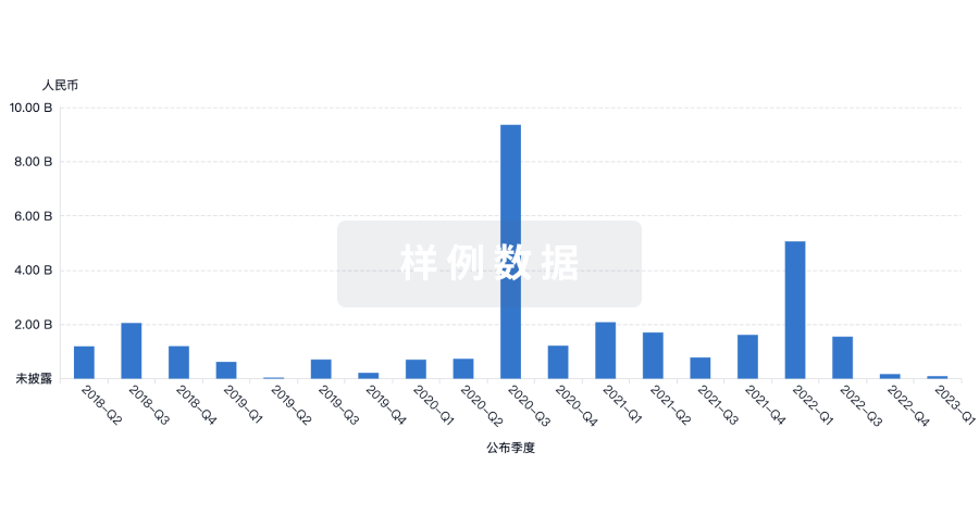
投资
深入了解从初创企业到成熟企业的最新公司投资动态。
登录
或
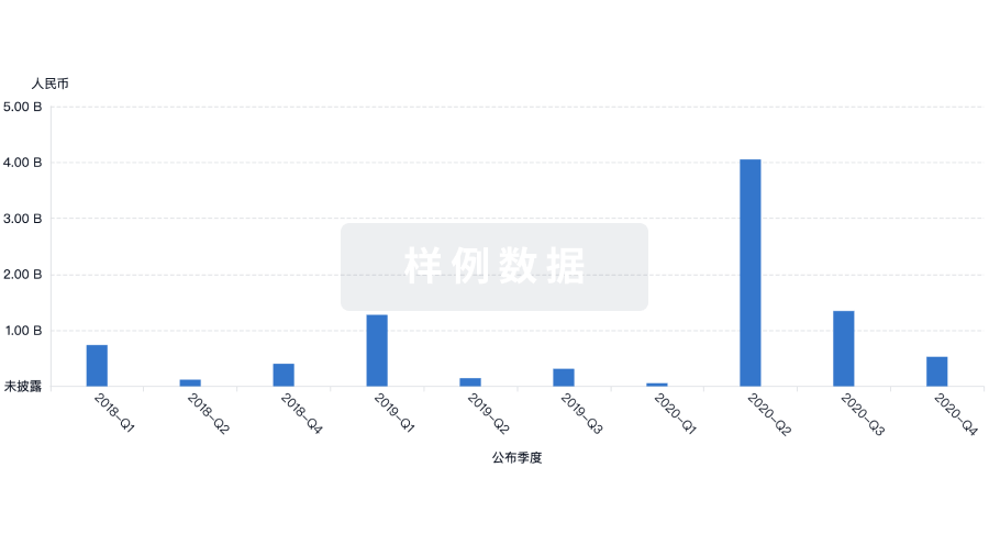
融资
发掘融资趋势以验证和推进您的投资机会。
登录
或
生物医药百科问答
全新生物医药AI Agent 覆盖科研全链路,让突破性发现快人一步
立即开始免费试用!
智慧芽新药情报库是智慧芽专为生命科学人士构建的基于AI的创新药情报平台,助您全方位提升您的研发与决策效率。
立即开始数据试用!
智慧芽新药库数据也通过智慧芽数据服务平台,以API或者数据包形式对外开放,助您更加充分利用智慧芽新药情报信息。
生物序列数据库
生物药研发创新
免费使用
化学结构数据库
小分子化药研发创新
免费使用


